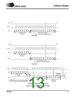
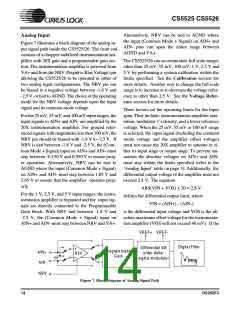
CS5525 CS5526
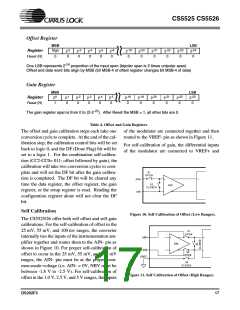
Offset Register
MSB
LSB
-2
-3
-4
-5
-6
-19
-20
-21
-22
-23
-24
Sign
Register
2
2
2
2
2
2
2
2
2
2
2
Reset (R)
0
0
0
0
0
0
0
0
0
0
0
0
-24
One LSB represents 2 proportion of the input span (bipolar span is 2 times unipolar span)
Offset and data word bits align by MSB (bit MSB-4 of offset register changes bit MSB-4 of data)
Gain Register
MSB
LSB
0
-1
-2
-3
-4
-5
-18
-19
-20
-21
-22
-23
Register
2
2
2
2
2
2
2
2
2
2
2
2
Reset (R)
1
0
0
0
0
0
0
0
0
0
0
0
-23
The gain register span is from 0 to (2-2 ). After Reset the MSB = 1, all other bits are 0.
Table 3.
Table 4. Offset and Gain Registers
The offset and gain calibration steps each take one
conversion cycle to complete. At the end of the cal-
ibration step, the calibration control bits will be set
back to logic 0, and the DF (Done Flag) bit will be
set to a logic 1. For the combination self-calibra-
tion (CC2-CC0= 011; offset followed by gain), the
calibration will take two conversion cycles to com-
plete and will set the DF bit after the gain calibra-
tion is completed. The DF bit will be cleared any
time the data register, the offset register, the gain
register, or the setup register is read. Reading the
configuration register alone will not clear the DF
bit.
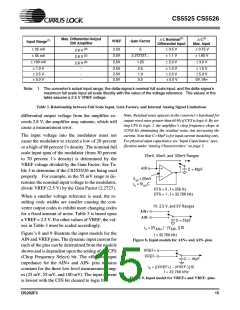
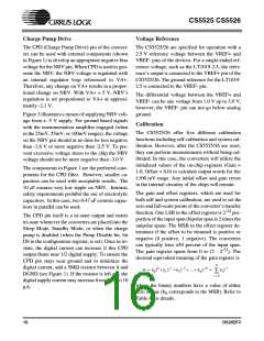
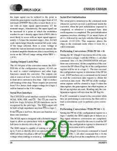
of the modulator are connected together and then
routed to the VREF- pin as shown in Figure 11.
For self-calibration of gain, the differential inputs
of the modulator are connected to VREF+ and
S 1
O P E N
A IN+
A IN -
+
-
+
-
S 2
C L O SE D
X 20
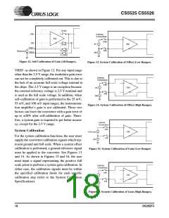
Self Calibration
Figure 10. Self Calibration of Offset (Low Ranges).
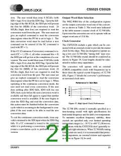
The CS5525/26 offer both self offset and self gain
calibrations. For the self-calibration of offset in the
25 mV, 55 mV, and 100 mv ranges, the converter
internally ties the inputs of the instrumentation am-
plifier together and routes them to the AIN- pin as
shown in Figure 10. For proper self-calibration of
offset to occur in the 25 mV, 55 mV, and 100 mV
ranges, the AIN- pin must be at the proper com-
mon-mode-voltage (i.e. AIN- = 0V, NBV must be
between -1.8 V to -2.5 V). For self-calibration of
offset in the 1.0 V, 2.5 V, and 5 V ranges, the inputs
S1
OPEN
AIN+
+
-
+
-
X20
AIN-
S2
O PEN
VREF-
S4
CLOSED
Figure 11. Self Calibration of Offset (High Ranges).
DS202F3
17

 CIRRUS [ CIRRUS LOGIC ]