CS5525 CS5526
O P E N
O P E N
A IN+
A IN -
+
-
+
-
External
Connections
X 20
+
-
+
-
AIN+
+
-
0V
X20
V RE F+
V RE F-
AIN-
+
+
-
C L O SE D
C L O SE D
Re fe re n ce
CM
-
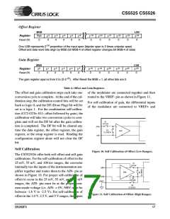
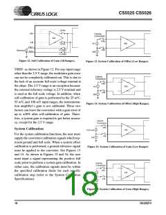
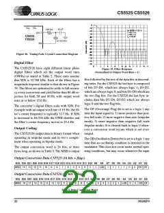
Figure 12. Self Calibration of Gain (All Ranges).
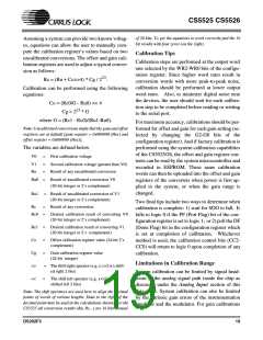
Figure 13. System Calibration of Offset (Low Ranges).
VREF- as shown in Figure 12. For any input range
other than the 2.5 V range, the modulator gain error
can not be completely calibrated out. This is due to
the lack of an accurate full scale voltage internal to
the chips. The 2.5 V range is an exception because
the external reference voltage is 2.5 V nominal and
is used as the full scale voltage. In addition, when
self-calibration of gain is performed in the 25 mV,
55 mV, and 100 mV input ranges, the instrumenta-
tion amplifier’s gain is not calibrated. These two
factors can leave the converters with a gain error of
up to 20ꢀ after self-calibration of gain. There-
fore, a system gain is required to get better accura-
cy, except for the 2.5 V range.
External
Connections
+
-
+
-
AIN+
AIN-
+
-
X20
0 V
+
-
CM
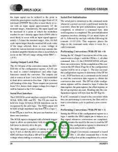
Figure 14. System Calibration of Offset (High Ranges).
External
C onnectio ns
+
-
+
-
A IN+
A IN -
System Calibration
+
-
X20
Full S cale
C M
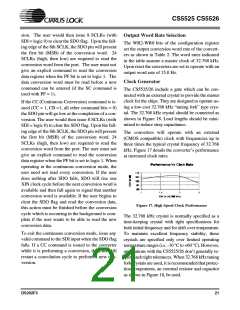
For the system calibration functions, the user must
supply the converters calibration signals which rep-
resent ground and full scale. When a system offset
calibration is performed, a ground reference signal
must be applied to the converter. See Figures 13
and 14. As shown in Figures 15 and 16, the user
must input a signal representing the positive full
scale point to perform a system gain calibration. In
either case, the calibration signals must be within
the specified calibration limits for each specific
calibration step (refer to the System Calibration
Specifications).
+
-
Figure 15. System Calibration of Gain (Low Ranges)
E xternal
C on nectio ns
+
-
+
-
A IN+
A IN -
+
-
X 20
Fu ll S ca le
C M
+
-
Figure 16. System Calibration of Gain (High Ranges).
18
DS202F3

 CIRRUS [ CIRRUS LOGIC ]