CS5525 CS5526
of 20 bits. To get the equations to work correctly pad the 16
bit results with four zeros (on the right).
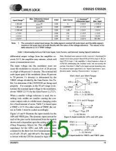
Assuming a system can provide two known voltag-
es, equations can allow the user to manually com-
pute the calibration register’s values based on two
uncalibrated conversions. The offset and gain cali-
bration registers are used to adjust a typical conver-
sion as follows:
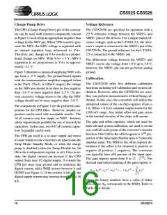
Calibration Tips
Calibration steps are performed at the output word
rate selected by the WR2-WR0 bits of the configu-
ration register. Since higher word rates result in
conversion words with more peak-to-peak noise,
calibration should be performed at lower output
word rates. Also, to minimize digital noise near
the devices, the user should wait for each calibra-
tion step to be completed before reading or writing
to the serial port.
23
Rc = (Ru + Co>>4) * Cg / 2 .
Calibration can be performed using the following
equations:
Co = (Rc0/G - Ru0) << 4
23
Cg = 2 * G
where G = (Rc1 - Rc0)/(Ru1-Ru0).
For maximum accuracy, calibrations should be per-
formed for offset and gain for each gain setting (se-
lected by changing the G2-G0 bits of the
configuration register). And if factory calibration is
performed using the system calibration capabilities
of the CS5525/26, the offset and gain register con-
tents can be read by the system microcontroller and
recorded in EEPROM. These same calibration
words can then be uploaded into the offset and gain
registers of the converters when power is first ap-
plied to the system, or when the gain range is
changed.
Note: Uncalibrated conversions imply that the gain and offset
registers are at default {gain register = 0x800000 (Hex) and
offset register = 0x000000 (Hex)}.
The variables are defined below.
V0
=
First calibration voltage
V1
Ru
=
=
Second calibration voltage (greater than V0)
Result of any uncalibrated conversion
Ru0
=
Result of uncalibrated conversion V0
(20-bit integer or 2’s complement)
Ru1
=
Result of uncalibrated conversion of V1
(20-bit integer or 2’s complement)
Two final tips include two ways to determine when
calibration is complete: 1) wait for SDO to fall. It
falls to logic 0 if the PF (Port Flag) bit of the con-
figuration register is set to logic 1; or 2) poll the DF
(Done Flag) bit in the configuration register which
is set at completion of calibration. Whichever
method is used, the calibration control bits (CC2-
CC0) will return to logic 0 upon completion of any
calibration.
Rc
=
=
Result of any conversion
Rc0
Desired calibration result of converting V0
(20-bit integer or 2’s complement)
Rc1
Co
Cg
>>
=
=
=
Desired calibration result of converting V1
(20-bit integer or 2’s complement)
Offset calibration register value (24-bit 2’s
complement)
Gain calibration register value
(24-bit integer)
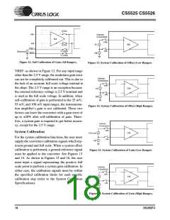
Limitations in Calibration Range
=
The shift right operator (e.g. x >>2 is x shift-
ed right 2 bits)
System calibration can be limited by signal head-
room in the analog signal path inside the chip as
discussed under the Analog Input section of this
data sheet. System calibration can also be limited
by the intrinsic gain errors of the instrumentation
amplifier and the modulator. For gain calibrations
<<
=
The shift left operator (e.g. x<<2 is x
shifted left 2 bits)
Note: The shift operators are used here to align the decimal
points of words of various lengths. Data to the right of the
decimal point may be used in the calculations shown. For the
CS5525 all conversion results (Ru, Rc...) are 16 bits instead
DS202F3
19

 CIRRUS [ CIRRUS LOGIC ]