CS5525 CS5526
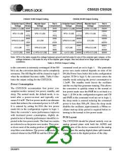
CS5525 16-Bit Output Coding
CS5526 20-Bit Output Coding
Unipolar Input Offset
Voltage Binary
Bipolar Input
Voltage
Two's
Complement
Unipolar Input Offset
Voltage Binary
Bipolar Input
Voltage
Two's
Complement
>(VFS-1.5 LSB) FFFF
>(VFS-1.5 LSB)
7FFF
>(VFS-1.5 LSB) FFFFF >(VFS-1.5 LSB)
7FFFF
FFFF
-----
FFFE
7FFF
-----
7FFE
FFFFF
-----
FFFFE
7FFFF
-----
7FFFE
VFS-1.5 LSB
VFS-1.5 LSB
VFS-1.5 LSB
VFS-1.5 LSB
-0.5 LSB
8000
-----
0000
-----
80000
-----
00000
-----
VFS/2-0.5 LSB
-0.5 LSB
VFS/2-0.5 LSB
7FFF
FFFF
7FFFF
FFFFF
0001
-----
8001
-----
00001
-----
80001
-----
+0.5 LSB
-VFS+0.5 LSB
+0.5 LSB
-VFS+0.5 LSB
0000
8000
00000
80000
<(+0.5 LSB)
0000
<(-VFS+0.5 LSB)
8000
<(+0.5 LSB)
00000 <(-VFS+0.5 LSB)
80000
Note: VFS in the table equals the voltage between ground and full scale for any of the unipolar gain ranges, or the
voltage between ± full scale for any of the bipolar gain ranges. See text about error flags under overrange
conditions.
Table 6. 5525/26 Output Coding
to the converters is extremely overranged. If the OD command word are set to logic 1. The particular
bit is set, the conversion data bits can be completely power save mode entered depends on state of bit
erroneous. The OD flag bit will be cleared to logic 0 D4 (the Power Save Select bit) in the configuration
when the modulator becomes stable. Table 6 illus-
trates the output coding for the CS5525/26.
register. If D4 is logic 0, the converters enters the
standby mode reducing the power consumption to
1.2mW. The standby mode leaves the oscillator
and the on-chip bias generator running. This allows
the converters to quickly return to the normal or
low power mode once the PS/R bit is set back to a
logic 1. If D4 in the configuration register and CB
and PS/R in the command word are set to logic 1,
the sleep mode is entered reducing the consumed
power to less than 500 µW. Since the sleep mode
disables the oscillator, approximately a 500ms os-
cillator start-up delay period is required before re-
turning to the normal or low power mode.
Power Consumption
The CS5525/26 accommodate four power con-
sumption modes: normal, low power, standby, and
sleep. The normal mode, the default mode, is en-
tered after a power-on-reset and typically con-
sumes 9.4 mW. The low power mode is an alternate
mode that reduces the consumed power to 4.9 mW.
It is entered by setting bit D16 (the low power
mode bit) in the configuration register to logic 1.
Since the converter’s noise performance improves
with increased power consumption, slightly de-
graded noise or linearity performance should be ex-
pected in the low power mode. The final two modes
are referred to as the power save modes. They pow-
PCB Layout
The CS5525/26 should be placed entirely over an
analog ground plane with both the AGND and
er down most of the analog portion of the chips and DGND pins of the device connected to the analog
stop filter convolutions. The power save modes are plane. Place the analog-digital plane split immedi-
entered whenever the PS/R bit and the CB bit of the ately adjacent to the digital portion of the chip.
DS202F3
23

 CIRRUS [ CIRRUS LOGIC ]