CS5525 CS5526
(1)
(1)
Max. Differential Output
20X Amplifier
∆-Σ Nominal
∆-Σ
(1)
VREF
Gain Factor
Input Range
Differential Input
Max. Input
(2)
± 25 mV
± 55 mV
± 100 mV
2.5V
2.5V
2.5V
5
± 0.5 V
± 0.75 V
2.8 V
(2)
2.272727...
1.25
± 1.1 V
± 2.0 V
± 1.65 V
± 3.0 V
2.8 V
(2)
2.8 V
± 1.0 V
± 2.5 V
± 5.0 V
-
-
-
2.5V
2.5V
2.5V
2.5
1.0
0.5
± 1.0 V
± 2.5 V
± 5.0 V
± 1.5 V
± 5.0 V
0V, VA+
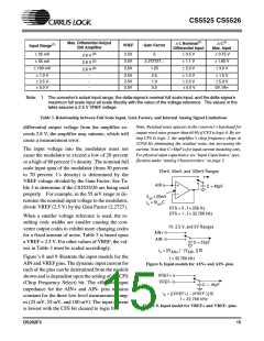
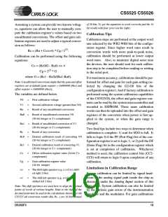
Note: 1. The converter's actual input range, the delta-sigma's nominal full scale input, and the delta-sigma's
maximum full scale input all scale directly with the value of the voltage reference. The values in the
table assume a 2.5 V VREF voltage.
Table 3. Relationship between Full Scale Input, Gain Factors, and Internal Analog Signal Limitations
Note: Residual noise appears in the converter’s baseband for
output word rates greater than 60 Hz if CFS is logic 0. By set-
ting CFS to logic 1, the amplifier’s chop frequency chops at
32768 Hz eliminating the residual noise, but increasing the
differential output voltage from the amplifier ex-
ceeds 2.8 V, the amplifier may saturate, which will
cause a measurement error.
The input voltage into the modulator must not
cause the modulator to exceed a low of 20 percent
or a high of 80 percent 1's density. The nominal full
scale input span of the modulator (from 30 percent
to 70 percent 1’s density) is determined by the
VREF voltage divided by the Gain Factor. See Ta-
ble 3 to determine if the CS5525/26 are being used
properly. For example, in the 55 mV range to de-
termine the nominal input voltage to the modulator,
divide VREF (2.5 V) by the Gain Factor (2.2727).
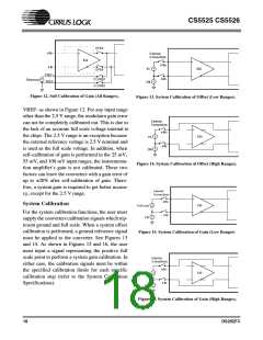
current. Note that C=48pF is for input current modeling only.
For physical input capacitance see ‘Input Capacitance’ spec-
ification under ‘Analog Characteristics’ on page 3.
25mV, 55mV, and 100mV Ranges
AIN
C = 48pF
V
i
25mV
≤
os
= fV
C
os
n
CFS = 0 , f = 256 Hz
CFS = 1 , f = 32.768 kHz
When a smaller voltage reference is used, the re-
sulting code widths are smaller causing the con-
verter output codes to exhibit more changing codes
for a fixed amount of noise. Table 3 is based upon
a VREF = 2.5 V. For other values of VREF, the val-
ues in Table 3 must be scaled accordingly.
1V, 2.5 V, and 5V Ranges
AIN+
AIN-
C = 32pF
i
= [(V
) - (V
)] fC
AIN -
n
AIN +
Figure’s 8 and 9 illustrate the input models for the
AIN and VREF pins. The dynamic input current for
each of the pins can be determined from the models
shown and is dependent upon the setting of the CFS
(Chop Frequency Select) bit. The effective input
impedance for the AIN+ and AIN- pins remains
constant for the three low level measurement rang-
es (25 mV, 55 mV, and 100 mV). The input current
is lowest with the CFS bit cleared to logic 0.
f = 32.768 kHz
Figure 8. Input models for AIN+ and AIN- pins
VREF+
VREF-
C = 16pF
i
= [(VREF+) - (VREF-)] fC
f = 32.768 kHz
n
Figure 9. Input model for VREF+ and VREF- pins.
DS202F3
15

 CIRRUS [ CIRRUS LOGIC ]