CS5525 CS5526
Alternatively, NBV can be tied to AGND where
the input (Common Mode + Signal) on AIN+ and
AIN- pins can span the entire range between
AGND and VA+.
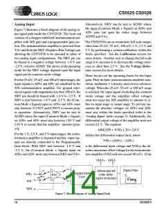
Analog Input
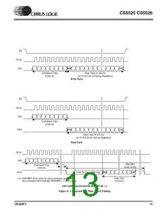
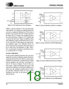
Figure 7 illustrates a block diagram of the analog in-
put signal path inside the CS5525/26. The front end
consists of a chopper-stabilized instrumentation am-
plifier with 20X gain and a programmable gain sec-
tion. The instrumentation amplifier is powered from
VA+ and from the NBV (Negative Bias Voltage) pin
allowing the CS5525/26 to be operated in either of
two analog input configurations. The NBV pin can
The CS5525/26 can accommodate full scale ranges
other than 25 mV, 55 mV, 100 mV, 1 V, 2.5 V and
5 V by performing a system calibration within the
limits specified. See the Calibration section for
more details. Another way to change the full scale
be biased to a negative voltage between -1.8 V and range is to increase or to decrease the voltage refer-
-2.5 V, or tied to AGND. The choice of the operating ence to other than 2.5 V. See the Voltage Refer-
mode for the NBV voltage depends upon the input
signal and its common mode voltage.
ence section for more details.
Three factors set the operating limits for the input
For the 25 mV, 55 mV, and 100 mV input ranges, the span. They include: instrumentation amplifier satu-
input signals to AIN+ and AIN- are amplified by the ration, modulator 1’s density, and a lower reference
20X instrumentation amplifier. For ground refer-
enced signals with magnitudes less then 100 mV, the
voltage. When the 25 mV, 55 mV or 100 mV range
is selected, the input signal (including the common
NBV pin should be biased with -1.8 V to -2.5 V. If mode voltage and the amplifier offset voltage)
NBV is tied between -1.8 V and -2.5 V, the (Com- must not cause the 20X amplifier to saturate in ei-
mon Mode + Signal) input on AIN+ and AIN- must ther its input stage or output stage. To prevent sat-
stay between -0.150 V and 0.950 V to ensure prop- uration the absolute voltages on AIN+ and AIN-
er operation. Alternatively, NBV can be tied to
AGND where the input (Common Mode + Signal)
must stay within the limits specified (refer to the
‘Analog Input’ table on page 3). Additionally, the
on AIN+ and AIN- must stay between 1.85 V and differential output voltage of the amplifier must not
2.65 V to ensure that the amplifier operates prop-
erly.
exceed 2.8 V. The equation
ABS(VIN + VOS) x 20 = 2.8 V
For the 1 V, 2.5 V, and 5 V input ranges, the instru-
mentation amplifier is bypassed and the input sig-
nals are directly connected to the Programmable
Gain block. With NBV tied between -1.8 V and
-2.5 V, the (Common Mode + Signal) input on
AIN+ and AIN- must stay between NBV and VA+.
defines the differential output limit, where
VIN = (AIN+) - (AIN-)
is the differential input voltage and VOS is the ab-
solute maximum offset voltage for the instrumenta-
tion amplifier (VOS will not exceed 40 mV). If the
VREF+ VREF-
D igital Filter
D ifferential 4th
order delta-
sigm a m odulator
Program m able
G ain
AIN +
AIN -
X 20
N BV
Figure 7. Block Diagram of Analog Signal Path
14
DS202F3

 CIRRUS [ CIRRUS LOGIC ]