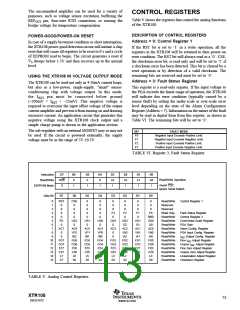
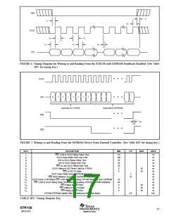
CS1
t7
t1
t5
SCLK
t2
t2
t3
t4
t6
DIO
FIGURE 6. Timing Diagram for Writing to and Reading From the XTR108 with EEPROM Readback Disabled. (See Table
XIV for timing key.)
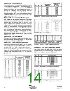
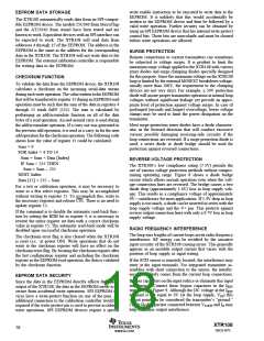
SCLK
0
1
1
1
1
1
1
1
DIO
Instruction to XTR108
Data to/from EEPROM
CS1
CS2
t14
FIGURE 7. Writing to and Reading From the EEPROM Device From External Controller. (See Table XIV for timing key.)
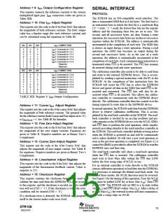
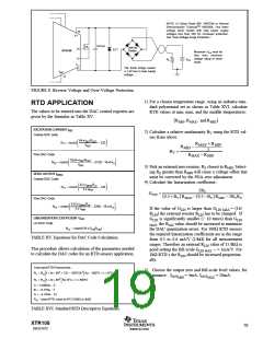
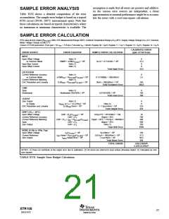
SPEC
DESCRIPTION
MIN
TYP
MAX
UNITS
t1
t2
CS1 LOW to SCLK Rising Setup Time
SCLK Pulse Width HIGH and LOW
2.0
100
20
20
20
0
ns
ns
ns
ns
ns
ns
ns
us
us
ns
us
ns
ns
ns
kHz
t3
DIO to SCLK Rising Setup Time
t4
DIO to SCLK Rising Hold Time
t5
CS1 to Last SCLK Rising Hold Time
t6
SCLK Falling to DIO Driven Valid by XTR108
CS1 to DIO Tri-State
50
20
t7
0
t8
SCLK Pulse Width During EEPROM Readback
CS2 HIGH Between Successive EEPROM Readbacks
SCLK Driven LOW Before CS1 LOW When Interrupting XTR108 Readback from EEPROM
CS1 LOW to SCLK Rising Setup Time When Interrupting XTR108 EEPROM Readback
CS1 Falling to CS2 HIGH
5
t9
10
t10
t11
t12
t13
t14
20
40
0
50
20
20
CS1 Falling to DIO Tri-State
0
CS1 Rising to CS2 HIGH
0
XTR108 EEPROM Update Rate in Continuous Readback Mode
0.9
TABLE XIV. Timing Diagram Key.
XTR108
SBOS187C
17
www.ti.com

 BB [ BURR-BROWN CORPORATION ]