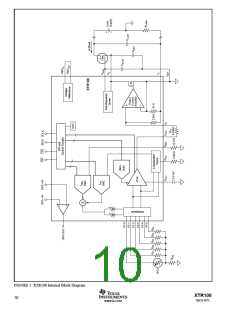
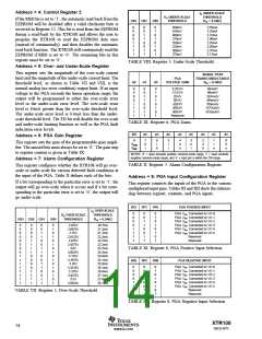
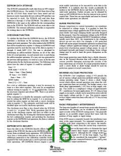
Address = 4: Control Register 2
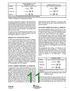
IO UNDER-SCALE
THRESHOLD
RVI = 6.34kΩ
VO UNDER-SCALE
THRESHOLD
If the RBD bit is set to ‘1’, the automatic read-back from the
EEPROM will be disabled after a valid checksum byte is
received in Register 15. This bit is read from the EEPROM
during a read-back by the XTR108 and allows the user to
program the XTR108 to read the EEPROM data once
(instead of continuously), and then disables the automatic
read-back function. The XTR108 will continuously read the
EEPROM if RBD is set to ‘0’. The remaining bits in this
register must be set to ‘0’.
US2
US1
US0
0
0
0
0
1
1
1
1
0
0
1
1
0
0
1
1
0
1
0
1
0
1
0
1
450mV
425mV
400mV
375mV
350mV
325mV
300mV
275mV
3.55mA
3.35mA
3.15mA
2.96mA
2.76mA
2.56mA
2.37mA
2.17mA
TABLE VIII. Register 5, Under-Scale Threshold.
Address = 5: Over- and Under-Scale Register
This register sets the magnitude of the over-scale current
limit and the magnitude of the under-scale current limit. The
threshold level, as shown in Table VII and VIII, is the
normal analog (no error condition) output limit. If an input
voltage to the PGA exceeds the linear operation range, the
output will be programmed to either the over-scale error
level or the under-scale error level. The over-scale error
level is 10mA greater than the over-scale threshold level.
The under-scale error level is 0.4mA less than the under-
scale threshold level. The FD bit will disable the over-scale
and under-scale limiting function as well as the PGA fault
indication error levels.
SIGNAL PATH
TRANSCONDUCTANCE
PGA
VOLTAGE GAIN
G2
G1
G0
RVI = 6.34kΩ
0
0
0
0
1
1
1
1
0
0
1
1
0
0
1
1
0
1
0
1
0
1
0
1
6.25V/V
12.5V/V
25V/V
49mA/V
99mA/V
197mA/V
394mA/V
789mA/V
1577mA/V
3155mA/V
50V/V
100V/V
200V/V
400V/V
Reserved
TABLE IX. Register 6, PGA Gains.
BIT
AC
AC
AC
AC
AC
AC
AC
AC
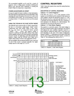
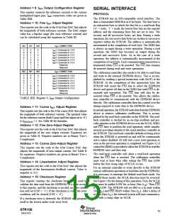
Address = 6: PGA Gain Register
#
VINN
VINP
7
h
l
6
l
h
5
l
l
4
h
h
3
n
l
2
n
h
1
l
n
0
h
n
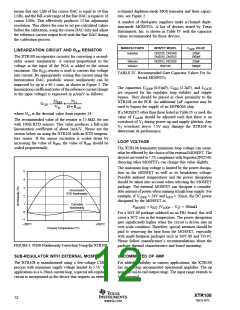
This register sets the gain of the programmable-gain ampli-
fier. The unused bits must always be set to ‘0’. The gain step
to register content is given in Table IX.
NOTES: ‘h’ = input exceeds positive common-mode range, ‘l’ = input exceeds
negative common-mode range, and ‘n’ = input pin is within the CM range.
Address = 7: Alarm Configuration Register
TABLE X. Register 7, Alarm Configuration Register.
This register configures whether the XTR108 will go over-
scale or under-scale for various detected fault conditions at
the input of the PGA. Table X defines each of the bits.
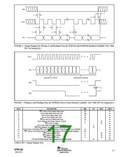
Address = 8: PGA Input Configuration Register
If a bit corresponding to the particular error is set to ‘1’, the
output will go over-scale when it occurs and if a bit corre-
sponding to the particular error is set to ‘0’, the output will
go under-scale.
This register connects the inputs of the PGA to the various
multiplexed input pins. Tables XI and XII show the relation-
ship between register, contents, and PGA inputs.
VP2
VP1
VP0
PGA POSITIVE INPUT
IO OVER-SCALE
0
0
0
0
1
1
1
1
0
0
1
1
0
0
1
1
0
1
0
1
0
1
0
1
PGA VIN+ Connected to V/ I-0
PGA VIN+ Connected to V/ I-1
PGA VIN+ Connected to V/ I-2
PGA VIN+ Connected to V/ I-3
PGA VIN+ Connected to V/I-4
PGA VIN+ Connected to V/I-5
Reserved
VO OVER-SCALE
THRESHOLD
THRESHOLD
OS3
OS2 OS1
OS0
RVI = 6.34kΩ
0
0
0
0
0
0
0
0
1
1
1
1
1
1
1
1
0
0
0
0
1
1
1
1
0
0
0
0
1
1
1
1
0
0
1
1
0
0
1
1
0
0
1
1
0
0
1
1
0
1
0
1
0
1
0
1
0
1
0
1
0
1
0
1
2.625V
2.6875V
2.75V
2.8125V
2.875V
2.9375V
3.0V
3.0625V
3.125V
3.1875V
3.25V
3.3125V
3.375V
3.4375V
3.5V
20.7mA
21.2mA
21.7mA
22.2mA
22.7mA
23.2mA
23.7mA
24.2mA
24.6mA
25.1mA
25.6mA
26.1mA
26.6mA
27.1mA
27.6mA
28.1mA
Reserved
TABLE XI. Register 8, PGA Positive Input Selection.
VN2
VN1
VN0
PGA NEGATIVE INPUT
0
0
0
0
1
1
1
1
0
0
1
1
0
0
1
1
0
1
0
1
0
1
0
1
PGA VIN– Connected to V/I-0
PGA VIN– Connected to V/I-1
PGA VIN– Connected to V/I-2
PGA VIN– Connected to V/I-3
PGA VIN– Connected to V/I-4
PGA VIN– Connected to V/I-5
Reserved
3.5625V
TABLE VII. Register 5, Over-Scale Threshold.
Reserved
TABLE XII. Register 8, PGA Negative Input Selection.
XTR108
14
SBOS187C
www.ti.com

 BB [ BURR-BROWN CORPORATION ]