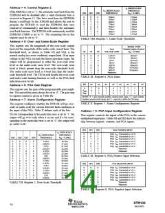
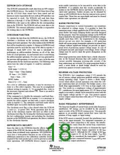
Address = 9: IREF Output Configuration Register
SERIAL INTERFACE
PROTOCOL
This register connects the reference currents to the various
multiplexed input pins. IREF connection codes are given in
Table XIII.
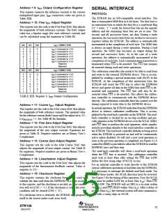
The XTR108 has an SPI-compatible serial interface. The
data is transmitted MSB first in 8-bit bytes. The first byte is
an instruction byte in which the first bit is a read/write flag
(‘0’ = write, ‘1’ = read), the lowest four bits are the register
address and the remaining three bits are set to zero. The
second, and all successive bytes, are data. During a write
operation, the successive data bytes are written to successive
registers within the XTR108. The address is automatically
incremented at the completion of each byte. The SDIO line
is always an input during a write operation. During a read
operation, the SDIO line becomes an output during the
second and successive bytes. As in the case of a write
operation, the address is automatically incremented at the
completion of each byte. Each communication transaction is
terminated when CS1 is de-asserted. The CS2 line remains
de-asserted during read and write operations.
Address = 10: Fine IREF Adjust Register
This register sets the code to the 8-bit Fine DAC that adjusts
the magnitude of both reference currents. The DAC output
value has a bipolar range (for each reference current) and
can be calculated using the equations in Table III.
IA2
IA1
IA0
IREF CONNECTION
0
0
0
0
1
1
1
1
0
0
1
1
0
0
1
1
0
1
0
1
0
1
0
1
IREF1 Connected to V/ I-0
I
I
REF1 Connected to V/ I-1
REF1 Connected to V/ I-2
I
I
REF1 Connected to V/ I-3
REF1 Connected to V/ I-4
IREF1 Connected to V/ I-5
Reserved
Reserved
IB2
IB1
IB0
IREF CONNECTION
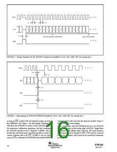
The calibration controller also needs to be able to read from
and write to the external EEPROM device. This is accom-
plished by sending a special instruction code (0x7F) to the
XTR108. At the completion of this instruction byte, the
XTR108 will assert the CS2 line to select the EEPROM
device and ignore all data on the SDIO line until CS1 is de-
asserted and reasserted. The CS2 line will also be de-
asserted when CS1 is de-asserted. This allows the calibra-
tion controller to communicate with the EEPROM device
directly. The calibration controller then has control over the
timing required to write data to the EEPROM device.
0
0
0
0
1
1
1
1
0
0
1
1
0
0
1
1
0
1
0
1
0
1
0
1
IREF2 Connected to V/ I-0
REF2 Connected to V/ I-1
REF2 Connected to V/ I-2
I
I
I
I
REF2 Connected to V/ I-3
REF2 Connected to V/ I-4
IREF2 Connected to V/ I-5
Reserved
Reserved
TABLE XIII. Register 9, IREF Output Configuration.
Address = 11: Coarse IREF Adjust Register
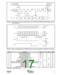
In normal operation, the XTR108 reads data from the EEPROM
device to retrieve calibration coefficients. This is accom-
plished by the read-back controller on the XTR108. The read-
back controller is clocked by an on-chip oscillator and pro-
vides stimulus to the EEPROM device over the SCLK, SDIO,
and CS2 lines to perform the read operation, while simulta-
neously providing stimulus to the serial interface controller in
the XTR108. The read-back controller defaults to being active
when the XTR108 is powered on and will be continuously
active unless disabled. (It will start a new read operation as
soon as the previous operation is completed, see Figure 4.) A
control bit (RBD) is provided to allow the XTR108 to read the
EEPROM once and then stop.
This register sets the code to the 8-bit coarse DAC that adjusts
the magnitude of both reference currents. The nominal value
for the reference current (both Coarse and Fine adjust set to ‘0’)
is IPROGRAM • 5. See Table III for formulas.
Address = 12: Fine Zero-Adjust Register
This register sets the code to the 8-bit Fine DAC that adjusts
the magnitude of the zero output currents. Equations are
given in Table II. Negative numbers are in Binary Two’s
Complement.
Address = 13: Coarse Zero-Adjust Register
This register sets the code to the 8-bit Coarse DAC that
adjusts the magnitude of zero-output current. See Table II
for equations. Negative numbers are given in Binary Two’s
Complement.
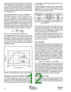
The read-back controller will abort a read-back operation
when the CS1 line is asserted. The calibration controller
must wait at least 40µs after setting the CS1 line LOW
before the first rising edge of SCLK occurs.
Address = 14: Linearization Adjust Register
This register sets the code to the 8-bit DAC that adjusts the
magnitude of the linearization feedback current. Value is
unipolar to 255.
For an external controller to write directly to the XTR108
(sensor calibration operation) or load data into the EEPROM,
it is necessary to interrupt the default read-back mode. For
both of these modes, the SCLK direction must be reversed.
See Figure 5 for the timing of this operation. First, the SCLK
line must be pulled LOW for at least 20ns (t10). Then CS1
is set LOW. The XTR108 will set DIO to a tri-state within
20ns (t13) and CS2 HIGH within 50ns (t12). After a delay of
at least 40µs (t11), the external system will start communica-
tion with a rising edge on SCLK.
Address = 15: Checksum Register
This register contains the checksum byte that is used to
validate the data read from the EEPROM. If a write occurs
to this register, and the checksum is invalid, an error condi-
tion will set (CSE = ‘1’). If the checksum is valid, the error
condition will be cleared (CSE = ‘0’).
If a checksum error is detected, the XTR108 will program
itself to the lowest under-scale error level.
XTR108
SBOS187C
15
www.ti.com

 BB [ BURR-BROWN CORPORATION ]