The uncommitted amplifier can be used for a variety of
purposes, such as voltage sensor excitation, buffering the
REFOUT pin, four-wire RTD connection, or sensing the
bridge voltage for temperature compensation.
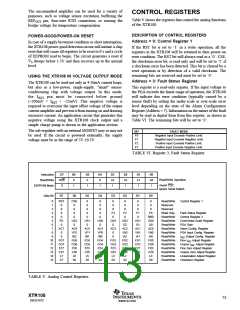
CONTROL REGISTERS
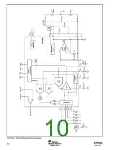
Table V shows the registers that control the analog functions
of the XTR108.
DESCRIPTION OF CONTROL REGISTERS
Address = 0: Control Register 1
POWER-GOOD/POWER-ON RESET
In case of a supply brownout condition or short interruption,
the XTR108 power-good detection circuit will initiate a chip
reset that will cause all registers to be reset to 0’s and a cycle
of EEPROM read to begin. The circuit generates a reset if
VS droops below 1.5V and then recovers up to the normal
level.
If the RST bit is set to ‘1’ in a write operation, all the
registers in the XTR108 will be returned to their power-on
reset condition. The RST bit will always read as a ‘0’. CSE,
the checksum error bit, is read only and will be set to ‘1’ if
a checksum error has been detected. This bit is cleared by a
reset operation or by detection of a valid checksum. The
remaining bits are reserved and must be set to ‘0’.
USING THE XTR108 IN VOLTAGE OUTPUT MODE
Address = 3: Fault Status Register
The XTR108 can be used not only in 4-20mA current loops,
but also as a low-power, single-supply, "smart" sensor-
conditioning chip with voltage output. In this mode,
the IRET pin must be connected below ground
(–200mV < IRET < –25mV). This negative voltage is
required to overcome the input offset voltage of the output
current amplifier and prevent it from turning on and drawing
excessive current. An application circuit that generates this
negative voltage using the XTR108 clock output and a
simple charge pump is shown in the application section.
This register is a read-only register. If the input voltage to
the PGA exceeds the linear range of operation, the XTR108
will indicate this error condition (typically caused by a
sensor fault) by setting the under-scale or over-scale error
level depending on the state of the Alarm Configuration
Register (Address = 7). Information on the nature of the fault
may be read in digital form from this register, as shown in
Table VI. The remaining bits will be set to ‘0’.
The sub-regulator with an external MOSFET may or may not
be used. If the circuit is powered externally, the supply
voltage must be in the range of 5V ±0.5V.
BIT
F0
F1
F2
F3
FAULT MODE
Negative Input Exceeds Positive Limit.
Negative Input Exceeds Negative Limit.
Positive Input Exceeds Positive Limit.
Positive Input Exceeds Negative Limit.
TABLE VI. Register 3, Fault Status Register.
Instruction
Read/Write
D7
R/W
0
D6
0
D5
0
D4
0
D3
A3
1
D2
A2
1
D1
A1
1
D0
A0
1
Read/Write Operation
Assert CS2
EEPROM Mode
1
1
1
Ignore Serial Data/A
Data Bit
D7
D6
D5
D4
D3
D2
D1
D0
0
1
RST
0
CSE
0
0
0
0
0
0
0
0
0
0
0
0
Read/Write
Reserved
Control Register 1
0
2
0
0
0
0
0
0
0
0
Reserved
3
0
0
0
0
F3
0
F2
F1
F0
Read Only
Read/Write
Read/Write
Read/Write
Read/Write
Read/Write
Read/Write
Read/Write
Read/Write
Read/Write
Read/Write
Read/Write
Read/Write
Fault Status Register
4
0
0
0
0
0
0
RBD
OS0
G0
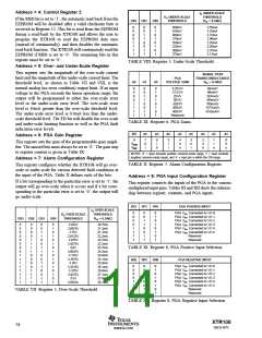
Control Register 2
5
FD
0
US2
0
US1
0
US0
0
OS3
0
OS2
G2
AC2
VN2
IA2
FG2
CG2
FZ2
CZ2
L2
OS1
G1
AC1
VN1
IA1
FG1
CG1
FZ1
CZ1
L1
Over/Under-Scale Register
PGA Gain
6
7
AC7
0
AC6
VP2
IB2
FG6
CG6
FZ6
CZ6
L6
AC5
VP1
IB1
FG5
CG5
FZ5
CZ5
L5
AC4
VP0
IB0
FG4
CG4
FZ4
CZ4
L4
AC3
0
AC0
VN0
IA0
FG0
CG0
FZ0
CZ0
L0
Alarm Config. Register
PGA Input Config. Register
IREF Output Config. Register
Fine IREF Adjust Register
Coarse IREF Adjust Register
Fine Zero Adjust Register
Coarse Zero Adjust Register
Linearization Adjust Register
Checksum Register
8
9
0
0
10
11
12
13
14
15
FG7
CG7
FZ7
CZ7
L7
S7
FG3
CG3
FZ3
CZ3
L3
S6
S5
S4
S3
S2
S1
S0
TABLE V. Analog Control Registers.
XTR108
SBOS187C
13
www.ti.com

 BB [ BURR-BROWN CORPORATION ]