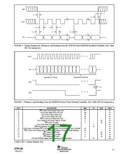
assumption is made that all errors are positive and additive.
As the various error sources are independent, a closer
approximation to nominal performance might be to accumu-
late the errors with a root-sum-square calculation.
SAMPLE ERROR ANALYSIS
Table XVII shows a detailed computation of the error
accumulation. The sample error budget is based on a typical
RTD circuit (Pt100, 200°C measurement span). Note that
these calculations are based on typical characteristics where
no maximum or minimum characteristic is available. The
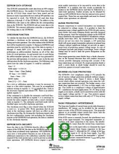
SAMPLE ERROR CALCULATION
RTD value at 4mA Output (RRTD MIN) 100Ω: RTD Measurement Range 200°C; Ambient Temperature Range (∆TA) 20°C; Supply Voltage Change (∆V+) 5V; Common-
Mode Voltage Change (∆CM) 0.1V.
Chosen XTR108 parameters: PGIA gain = 50; IREF = 518.9µA; Full-scale VIN = 40mW. Register 06 = 0H03; Register 11 = 0H11; Register 13 = 0HFC; Register 14 = 0H70.
CALIBRATED ERROR
ERROR SOURCE
ERROR EQUATION
SAMPLE ERROR CALCULATION
(ppm of Full Scale)
INPUT
Input Offset Voltage
vs Common Mode
Input Bias Current
Input Offset Current
Note (1)
CMRR • ∆CM/(VIN MAX) • 106
Note (1)
0
12.5
0
5µV/V • 0.1V/0.04V • 106
Note (1)
0
Total Input Error:
12.5
EXCITATION
Current Reference Accuracy
vs Common Mode
Current Reference Matching
DAC Resolution and Linearity
Note (1)
0
2.5
∆CM/ROUT • RRTD MIN/(VIN MAX) • 106
Note (1)
0.1V/100MΩ • 100Ω/40mV
1LSBFINE • RRTD MIN/(VIN MAX) • 106
96nA • 100Ω/40mV • 106
240
Total Excitation Error:
242.5
GAIN
Span
Nonlinearity
Note (1)
Nonlinearity (%)/100% • 106
0
100
100
0.01%/100% • 106
Total Gain Error:
OUTPUT
Zero Output
vs Supply
DAC Resolution and Linearity
Note (1)
(IZERO vs V+) • ∆V+/16mA • 106
2LSBFINE/16mA • 106
0
6
225
231
Note (2)
2 • 1.8µA/16mA • 106
Total Output Error:
DRIFT (∆TA = 20°C)
Input Offset Voltage
Current Reference Accuracy
Current Reference Matching
Span
Drift • ∆TA/(VIN MAX) • 106
Drift • ∆TA
Drift • ∆TA • IREF • RRTD MIN/(VIN MAX
0.02µV/°C • 20°C/40mV • 106
35ppm • 20°C
15ppm • 20°C • 518.9µA • 100/40mV
30ppm • 20°C
10
700
390
600
250
1950
)
Drift • ∆TA
Drift • ∆TA
Zero Output
Note (1)
Total Drift Error:
NOISE (0.1Hz to 10Hz, Typ)
Input Offset Voltage
Current Reference
Zero Output
VN/(VIN MAX) • 106
IREF Noise • RRTD MIN/(VIN MAX) • 106
IZERO Noise/16mA • 106
6µV/40mV • 106
0.015µA • 100Ω/40mV • 106
1.1µA/16mA • 106
150
37.5
68.5
256
Total Noise Error:
TOTAL ERROR:
2792 (1997)(3)
0.28% (0.20%)(3)
NOTES: (1) Does not contribute to the output error due to calibration. (2) All errors are referred to input unless otherwise stated. (3) Calculated as root-
sum–square.
TABLE XVII. Sample Error Budget Calculation.
XTR108
SBOS187C
21
www.ti.com

 BB [ BURR-BROWN CORPORATION ]