6) Choose PGA gain from the available list and calculate
the initial excitation current using:
Step 3.
• Calculate corrections using the following equations:
I
– IMEAS1 R
VI
(
=
)
MEAS2
I
– I
• 1– G
R
– RZ • R
MAX VI
(
)
(
)
(
)
I
OUTMAX
OUTMIN
LIN
REFA
50APGA
R
– RMIN
MAX
IREF
=
(
)
1,2
50 • APGA • R
– RMIN
(
)
MAX
I
– IMEAS1 R
(
)
ZERO
VI
RZ = RMIN
+
A
50APGAIREFA
Important: the PGA gain value should be chosen such
that the IREF value is within ±35% of 5VREF/RSET to
allow room for calibration adjustments without having
to go to another span step.
2BV
GLINA
=
0.5 + B
R
– 0.5 – B
R
– 2BVRZA
MIN
(
)
(
)
V
MAX
V
I
(
– I OUT
• 1– G
R
– RZA • RVI
7) The required DAC zero offset current value can be
calculated by:
)
(
)
OUT
MAX
(
LIN_ A
MAX
)
MIN
IREF
=
B
50 • APGA • R
– RMIN
(
)
MAX
∆IREF = I
– IREF + I
– IREF
REF
B
(
)
(
)
REF
A
50 • APGAIREF
R
– RZ
MIN
(
)
IZERO = I
–
OUTMIN
1024 • ∆IREFRSET
RVI
Adjusted IREF fine DAC Code : N10 = N10 + round
A
VREF
50 • APGA REF
I
R
(
MIN – RZA
Example:
)
B
∆IZERO = IOUT
– IZERO –
MIN
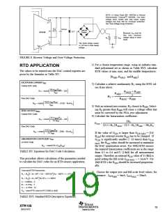
Measurement Range: TMIN = –20°C, TMAX = 50°C; 100Ω
RVI
RTD.
512 • ∆IZERORVI
5 • VREF
Adjusted IZERO fine DAC Code : N12 = N12 + round
A
1) RMIN = 92.16Ω, RMAX = 119.40Ω, RMID = 105.85Ω;
2) Sensor relative nonlinearity: BV = 0.0026;
3) Choosing RZ = 90.9Ω (closest to RMIN 2% value);
4) Linearization coefficient: GLIN = 0.3804mA/V;
5) 4-20mA output span;
This takes into account resistor value deviations, all
offsets and gain errors of the coarse DACs and PGA. If
the adjusted abs(N12A) > 128 or abs(N10A) > 128, adjust
the coarse DAC first, then recalculate the fine DAC
value;
6) PGA voltage gain APGA = 200, sensor excitation current
IREF1,2 = 368.39mA;
• Update all the DAC register value, including lineariza-
tion DAC.
7) Zero offset DAC: IZERO = 3.268mA
Step 4 (optional).
Measure output signal IMEAS3 with maximum RTD value
still connected to the input from step 2;
CALIBRATION PROCEDURE FOR RTD SENSORS
Step 1 Initial parameters calculation.
• Using the procedure above, compute IREF, APGA, IZERO
,
Step 5 (optional).
and GLIN based on TMIN, TMAX, and nominal values of
RZ, RSET, and RVI. Use the equation in Table XV to
calculate the DAC register values.
Compute GLIN correction and update LinDAC register;
Step 6 (optional).
Make verification measurements at min- and max-input
signal; If linearity check is needed: make a measurement at
mid-scale; write EEPROM data.
• Configure the input MUX, write PGA gain, reference,
and offset DAC registers of the XTR108 with calcu-
lated settings. Note: write GLIN = 0 (no linearization) to
XTR108 at this step;
Step 7.
Set the desired over-scale, under-scale signal limits and
sensor burnout indication configuration. Verify and adjust
the over-scale and under-scale levels by applying the posi-
tive and negative overdriving differential signals to the PGA
inputs.
Step 2 Measurement.
• Set RTD resistor value (or oven temperature) to mini-
mum scale, measure output signal IMEAS1
• Set RTD resistor value (or oven temperature) to maxi-
mum scale, measure output signal IMEAS2
;
;
XTR108
20
SBOS187C
www.ti.com

 BB [ BURR-BROWN CORPORATION ]