means that one LSB of the coarse DAC is equal to 16 fine
LSBs, and the full-scale range of the fine DAC is equal to 16
coarse LSBs. This effectively produces 12-bit adjustment
resolution. This allows the user to set pre-calculated values
before the calibration, using the coarse DAC only and adjust
the reference current output level with the fine DAC during
the calibration process.
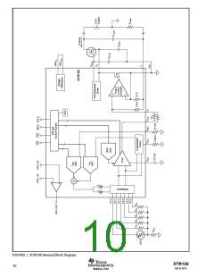
n-channel depletion-mode MOS transistor and three capaci-
tors, see Figure 2.
A number of third-party suppliers make n-channel deple-
tion-mode MOSFETs. A list of devices tested by Texas
Instruments, Inc. is shown in Table IV with the capacitor
values recommended for those devices.
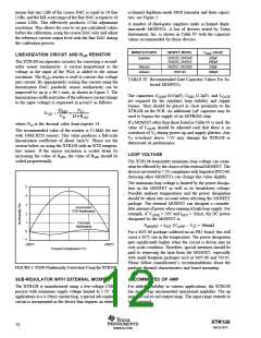
MANUFACTURER
MOSFET MODEL
CGATE VALUE
LINEARIZATION CIRCUIT AND RLIN RESISTOR
Supertex
DN2535, DN2540
DN3535, DN3525
220pF
1000pF
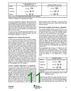
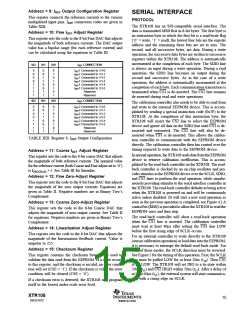
The XTR108 incorporates circuitry for correcting a second-
order sensor nonlinearity. A current proportional to the
voltage at the input of the PGA is added to the sensor
excitation. The RLIN resistor is used to convert this voltage
into current. By appropriately scaling this current using the
linearization DAC, parabolic sensor nonlinearity can be
improved by up to a 40:1 ratio, as shown in Figure 3. The
linearization coefficient (ratio of the reference current change
to the input voltage) is expressed in µA/mV as follows:
Siliconix
Infineon
ND2012, ND2020
BSP149
220pF
1000pF
TABLE IV. Recommended Gate Capacitor Values For Se-
lected MOSFETs.
The capacitors CLOOP (0.01µF), CREG (2.2µF), and CGATE
are required for the regulator loop stability and supply
bypass. They should be placed in close proximity to the
XTR108 on the PCB. An additional 1µF capacitor may be
used to bypass the supply of an EEPROM chip.
∆IREF
N14
GLIN
=
•
VIN 16 • RLIN
If a MOSFET other than those listed in Table IV is used, the
value of CGATE should be adjusted such that there is no
overshoot of VS during power-up and supply glitches. Any
VS overshoot above 7.5V may damage the XTR108 or
deteriorate its performance.
where N14 is the decimal value from register 14.
The recommended value of the resistor is 15.8kΩ, for use
with 100Ω RTD sensors. This value produces a full-scale
linearization coefficient of about 1mA/V. Please see the
section below on using the XTR108 with an RTD tempera-
ture sensor. If the sensor excitation is scaled down by
increasing the value of RSET, the value of RLIN should be
scaled proportionally.
LOOP VOLTAGE
The XTR108 transmitter minimum loop voltage can some-
what be effected by the choice of the external MOSFET. The
devices are tested to 7.5V compliance with Supertex DN2540;
choosing other MOSFETs can change this value slightly.
The maximum loop voltage is limited by the power dissipa-
tion on the MOSFET as well as its breakdown voltage.
Possible ambient temperatures and the power dissipation
should be taken into account when selecting the MOSFET
package. The external MOSFET can dissipate a consider-
able amount of power when running at high loop supply. For
example, if VLOOP = 24V and IOUT = 20mA, the DC power
dissipated by the MOSFET is:
5
4
3
Uncorrected
RTD Nonlinearity
2
Corrected
Nonlinearity
1
0
PMOSFET = IOUT (VLOOP – VS) = 380mΩ
For a SOT-89 package soldered on an FR5 board, this will
cause a 30°C rise in the temperature. The power dissipation
gets significantly higher when the circuit is driven into an
over-scale condition. Therefore, special attention should be
paid to removing the heat from the MOSFET, especially
with small-footprint packages such as SOT-89 and TO-92.
Please follow manufacturer’s recommendations about the
package thermal characteristics and board mounting.
–1
–200°C
+850°C
Process Temperature (°C)
FIGURE 3. Pt100 Nonlinearity Correction Using the XTR108.
SUB-REGULATOR WITH EXTERNAL MOSFET
UNCOMMITTED OP AMP
The XTR108 is manufactured using a low-voltage CMOS
process with maximum supply voltage limited to 5.5V. For
applications in a 4-20mA current loop, a special sub-regulator
circuit is incorporated in the device that requires an external
For added flexibility in various applications, the XTR108
has an on-chip uncommitted operational amplifier. The op
amp has rail-to-rail output range. The input range extends to
IRET potential.
XTR108
12
SBOS187C
www.ti.com

 BB [ BURR-BROWN CORPORATION ]