TSC2005
www.ti.com
SBAS379–DECEMBER 2006
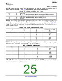
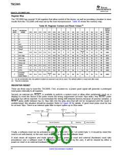
Table 18. Sense Time Selection
SNS2
SNS1
SNS0
SENSE TIME (tSNS)
0
0
0
0
1
1
1
1
0
0
1
1
0
0
1
1
0
1
0
1
0
1
0
1
32µs
96µs
544µs
608µs
2.080ms
2.144ms
2.592ms
2.656ms
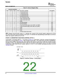
DTW—Detection of pen touch in wait. Writing a '1' to this bit enables the pen touch detection in background
while waiting for the host to issue the converter function in host-initiated/controlled modes. This detection in
background allows the TSC2005 to pull high at PINTDAV to indicate no pen touch detected while waiting for the
host to issue the converter function. If the host polls a high state at PINTDAV before the convert function is sent,
the host can abort the issuance of the convert function and stay in the polling PINTDAV mode until the next pen
touch is detected.
LSM—Longer sampling mode. When this bit is set to '1', the extra 500ns of sampling time is added to the
normal sampling cycles of each conversion. This additional time is represented as approximatly two A/D
converter clock cycles set by CL1-CL0.
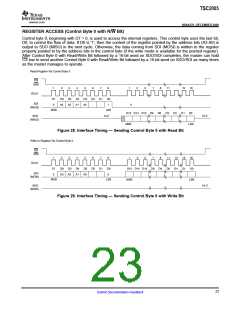
Configuration Register 1
Configuration register 1 (CFR1) defines the connection test-bit modes configuration and the batch delay
selection.
Table 19. Configuration Register 1 (Reset Value = 0000h)
MSB
D15
LSB
D0
D14
D13
D12
D11
D10
D9
D8
D7
D6
D5
D4
D3
D2
D1
Resrvd Resrvd Resrvd Resrvd TBM3 TBM2 TBM1 TBM0
Resrvd
Resrvd
Resrvd
Resrvd
Resrvd
BTD2
BTD1
BTD0
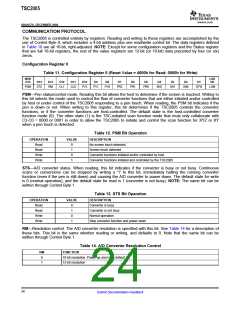
TBM3-TBM0—Connection test-bit modes. These bits specify the mode of test bits used for the predefined range
of touch screen panel resistance.
Table 20. Touch Screen Resistance Range and Test-Bit Modes
TEST-BIT MODES
RTS
TBM3
TBM2
TBM1
TBM0
(kΩ)
0
0
0
0
0
0
0
0
1
1
1
1
1
1
1
1
0
0
0
0
1
1
1
1
0
0
0
0
1
1
1
1
0
0
1
1
0
0
1
1
0
0
1
1
0
0
1
1
0
1
0
1
0
1
0
1
0
1
0
1
0
1
0
1
0.17
0.17 < RTS ≤ 0.52
0.52 < RTS ≤ 0.86
0.86 < RTS ≤ 1.6
1.6 < RTS ≤ 2.2
2.2 < RTS ≤ 3.6
3.6 < RTS ≤ 5.0
5.0 < RTS ≤ 7.8
7.8 < RTS ≤ 10.5
10.5 < RTS ≤ 16.0
16.0 < RTS ≤ 21.6
21.6 < RTS ≤ 32.6
Reserved
Reserved
Reserved
Only for short-circuit panel test
26
Submit Documentation Feedback

 BB [ BURR-BROWN CORPORATION ]