TSC2005
www.ti.com
SBAS379–DECEMBER 2006
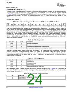
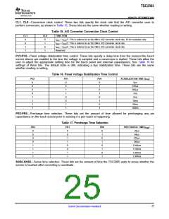
CL1, CL0—Conversion clock control. These two bits specify the clock rate that the A/D converter uses to
perform conversion, as shown in Table 15. These bits are the same whether reading or writing.
Table 15. A/D Converter Conversion Clock Control
CL1
0
CL0
0
FUNCTION
fADC = fOSC/1. This is referred to as the 4MHz A/D converter clock rate, 10-bit resolution only.
fADC = fOSC/2. This is referred to as the 2MHz A/D converter clock rate.
fADC = fOSC/4. This is referred to as the 1MHz A/D converter clock rate.
Reserved
0
1
1
0
1
1
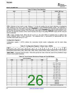
PV2-PV0—Panel voltage stabilization time control. These bits specify a delay time from the moment the touch
screen drivers are enabled to the time the voltage is sampled and a conversion is started. These bits allow the
user to adjust the appropriate settling time for the touch panel and external capacitances. See Table 16 for
settings of these bits. The default state is 000, indicating a 0µs stabilization time. These bits are the same
whether reading or writing.
Table 16. Panel Voltage Stabilization Time Control
PV2
0
PV1
0
PV0
0
STABILIZATION TIME (tPVS)
0µs
100µs
500µs
1ms
0
0
1
0
1
0
0
1
1
1
0
0
5ms
1
0
1
10ms
50ms
100ms
1
1
0
1
1
1
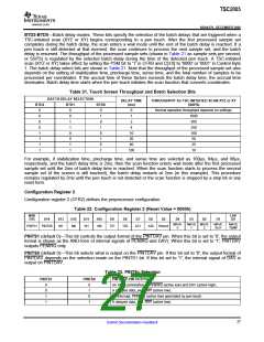
PR2-PR0—Precharge time selection. These bits set the amount of time allowed for precharging any pin
capacitance on the touch screen prior to sensing if a pen touch is happening.
Table 17. Precharge Time Selection
PR2
0
PR1
0
PR0
0
PRECHARGE TIME(tPRE)
20µs
84µs
0
0
1
0
1
0
276µs
0
1
1
340µs
1
0
0
1.044ms
1.108ms
1.300ms
1.364ms
1
0
1
1
1
0
1
1
1
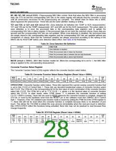
SNS2-SNS0—Sense time selection. These bits set the amount of time the TSC2005 waits to sense whether the
screen is touched after converting a coordinate.
25
Submit Documentation Feedback

 BB [ BURR-BROWN CORPORATION ]