TSC2005
www.ti.com
SBAS379–DECEMBER 2006
Register Map
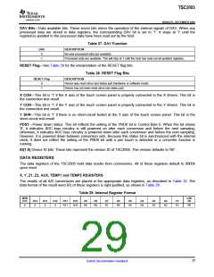
The TSC2005 has several 16-bit registers that allow control of the device, as well as providing a location to store
results from the TSC2005 until read out by the host microprocessor. Table 30 shows the memory map.
Table 30. Register Content and Reset Values(1)
RESET
A3-A0
(HEX)
REGISTER
NAME
VALUE
(HEX)
D15
0
D14
0
D13
0
D12
0
D11
R11
R11
R11
R11
R11
R11
R11
D10
R10
R10
R10
R10
R10
R10
R10
D9
R9
R9
R9
R9
R9
R9
R9
D8
R8
R8
R8
R8
R8
R8
R8
D7
R7
R7
R7
R7
R7
R7
R7
D6
R6
R6
R6
R6
R6
R6
R6
D5
R5
R5
R5
R5
R5
R5
R5
D4
R4
R4
R4
R4
R4
R4
R4
D3
R3
R3
R3
R3
R3
R3
R3
D2
R2
R2
R2
R2
R2
R2
R2
D1
R1
R1
R1
R1
R1
R1
R1
D0
R0
R0
R0
R0
R0
R0
R0
0
1
2
3
4
5
6
X
Y
0000
0000
0000
0000
0000
0000
0000
0
0
0
0
Z1
0
0
0
0
Z2
0
0
0
0
AUX
Temp1
Temp2
0
0
0
0
0
0
0
0
0
0
0
0
Rsvd
7
Status
S15
S14
S13
S12
S11
S10
S9
0
S7
S6
S5
S3
S2
S1
S0
0004
(2)
8
9
AUX High
AUX Low
Temp High
Temp Low
CFR0
0
0
0
0
0
0
0
0
R11
R11
R11
R11
R11
R11
R11
R10
R10
R10
R10
R10
R10
R10
R9
R9
R9
R9
R9
R9
R9
R8
R8
R8
R8
R8
R8
R8
R7
R7
R7
R7
R7
0
R6
R6
R6
R6
R6
0
R5
R5
R5
R5
R5
0
R4
R4
R4
R4
R4
0
R3
R3
R3
R3
R3
0
R2
R2
R2
R2
R2
R2
R2
R1
R1
R1
R1
R1
R1
R1
R0
R0
R0
R0
R0
R0
R0
0FFF
0000
0FFF
0000
4000
0000
0000
A
B
C
D
E
0
0
0
0
0
0
0
0
R15
0
R14
0
R13
0
R12
0
CFR1
CFR2
R15
R14
R13
R12
R7
R6
0
R4
R3
Converter
Function
Rsvd
F
R15
R14
R13
R12
R10
R9
R8
R7
R6
R5
R4
R3
R2
R1
R0
0000
(2)
Select Status
(1) For all combination bits, the pattern marked as reserved must not be used. The default pattern is read back after reset.
(2) This bit is reserved.
REGISTER RESET
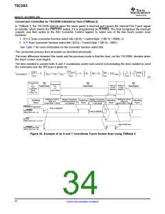
There are three way to reset the TSC2005. First, at power-on, a power good signal will generate a prolonged
reset pulse internally to all registers.
Second, an external pin, RESET, is available to perform a system reset or allow other peripherals (such as a
display) to reset the device if the pulse meets the timing requirement (at least 10µs wide). Any RESET pulse
less than 5µs will be rejected. To accommodate the timing drift between devices because of process variation, a
RESET pulse width between 5µs to 10µs falls into the gray area that will not be recognized and the result is
undetermined; this situation should be avoided. Refer to Figure 30 for details. A good reset pulse must be low
for at least 10µs. There is an internal spike filter to reject spikes up to 20ns wide.
tR
tR
tWL(RESET) < 5ms
tWL(RESET) ³ 10ms
RESET
State
Normal Operation
Resetting
Initial Condition
Figure 30. External Reset Timing
Finally, a software reset can be activated by writing a '1' to CB1.1 (bit 1 of control byte 1). It should be noted this
reset is not self-cleared, so the user must write a '0' to remove the software reset.
A reset clears all registers and loads default values. A power-on reset and external (hardware) reset take
precedence over a software reset. If a software reset not cleared by the user, it will be cleared by either a
power-on reset or an external (hardware) reset.
30
Submit Documentation Feedback

 BB [ BURR-BROWN CORPORATION ]