TSC2005
www.ti.com
SBAS379–DECEMBER 2006
DAV Bits—Data available bits. These seven bits mirror the operation of the internal signals of DAV. When any
processed data are stored in data registers, the corresponding DAV bit is set to '1'. It stays at '1' until the
register(s) updated to the processed data have been read out by the host.
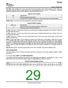
Table 27. DAV Function
DAV
DESCRIPTION
0
1
No new processed data are available.
Processed data are available. This will stay at 1 until the host has read out all updated registers.
RESET Flag—See Table 28 for the interpretation of the RESET flag bits.
Table 28. RESET Flag Bits
RESET Flag
DESCRIPTION
0
1
Device was reset since last status poll (hardware or software reset).
Device has not been reset since last status poll.
X CON—This bit is '1' if the X axis of the touch screen panel is properly connected to the X drivers. This bit is
the connection test result.
Y CON—This bit is '1' if the Y axis of the touch screen panel is properly connected to the Y drivers. This bit is
the connection test result.
Y SHR—This bit is '1' if there is no short-circuit tested at the Y axis of the touch screen panel. This bit is the
short-circuit test result.
PDST—Power down status. This bit reflects the setting of the PND0 bit in Control Byte 0. When this bit shows
'0', it indicates ADC bias circuitry is still powered on after each conversion and before the next sampling;
otherwise, it indicates ADC bias circuitry is powered down after each conversion and before the next sampling.
However, it is powered down between conversion sets. Because this status bit is synchronized with the internal
clock, it does not reflect the setting of the PND0 bit until a pen touch is detected or a converter function is
running.
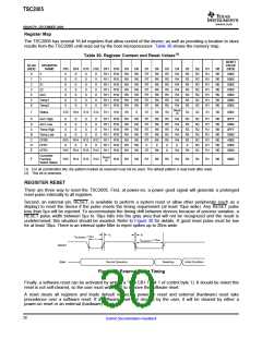
ID[1:0] Device ID bits: These bits represent the version ID of TSC2005. This version defaults to '00'.
DATA REGISTERS
The data registers of the TSC2005 hold data results from conversions. All of these registers default to 0000h
upon reset.
X, Y, Z1, Z2, AUX, TEMP1 and TEMP2 REGISTERS
The results of all A/D conversions are placed in the appropriate data registers, as described in Table 10. The
data format of the result word (R) of these registers is right-justified, as shown in Table 29:
Table 29. Internal Register Format
MSB
D15
LSB
D0
D14
D13
D12
D11
D10
D9
D8
D7
D6
D5
D4
D3
D2
D1
0
0
0
0
R11
R10
R9
R8
R7
R6
R5
R4
R3
R2
R1
R0
29
Submit Documentation Feedback

 BB [ BURR-BROWN CORPORATION ]