TSC2005
www.ti.com
SBAS379–DECEMBER 2006
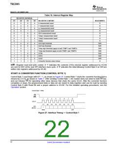
Table 10. Internal Register Map
REGISTER ADDRESS
A3
0
0
0
0
0
0
0
0
1
1
1
1
1
1
1
1
A2
0
0
0
0
1
1
1
1
0
0
0
0
1
1
1
1
A1
0
0
1
1
0
0
1
1
0
0
1
1
0
0
1
1
A0
0
1
0
1
0
1
0
1
0
1
0
1
0
1
0
1
REGISTER CONTENT
READ/WRITE
X measurement result
Y measurement result
Z1 measurement result
Z2 measurement result
AUX measurement result
Temp1 measurement result
Temp2 measurement result
Status
R
R
R
R
R
R
R
R
AUX high threshold
R/W
R/W
R/W
R/W
R/W
R/W
R/W
R
AUX low threshold
Temp high threshold (apply to both TEMP1 and TEMP2)
Temp low threshold (apply to both TEMP1 and TEMP2)
CFR0
CFR1
CFR2
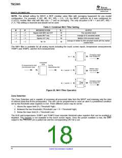
Converter function select status
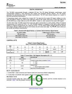
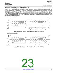
R/W—Register read and write control. A '1' indicates the contents of the internal register addressed by A3-A0
are sent to SDO at the next SPI interface clock cycle. A '0' indicates the data following Control Byte 0 on SDI are
written into registers addressed by A3-A0.
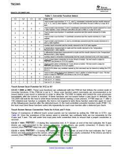
START A CONVERTER FUNCTION (CONTROL BYTE 1)
Control Byte 1 must begin with D7 = 1, as shown in Figure 27. Control Byte 1 starts the converter function that is
chosen by C3-C0, as shown in Table 7. After sending Control Byte 1, the master does not need to hold CS low,
and can release CS for operating other slave devices that share the same SCLK. After the converter function
completes or stops, the preprocessed data or data set are stored in data registers and can be read by sending
Control Byte 0 with Read Bit and a proper address in A3-A0. For the detailed operating procedures, see the
Operation section.
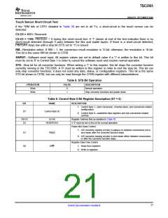
Control Byte 1 Write
CS
(SS)
1
2
3
4
5
6
7
8
SCLK
D7
D5
D4
D3
D2
D1
D0
D6
SDI
1
(MOSI)
MSB
LSB
Figure 27. Interface Timing — Control Byte 1
22
Submit Documentation Feedback

 BB [ BURR-BROWN CORPORATION ]