PCM1804
SLES022A – DECEMBER 2001
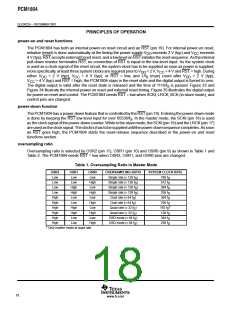
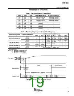
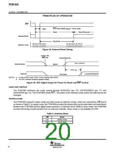
PRINCIPLES OF OPERATION
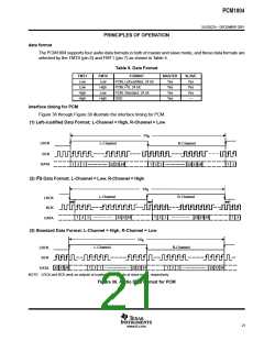
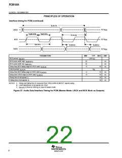
interface timing for PCM (continued)
t
(LRCP)
0.5 V
0.5 V
0.5 V
LRCK
DD
DD
DD
t
t
w(BCKL)
w(BCKH)
t
(CKLR)
BCK
DATA
t
(BCKP)
t
t
(LRDO)
(CKDO)
PARAMETERS
MIN
TYP
1/(64 f )
MAX
UNIT
BCK period, t
(BCKP)
S
BCK pulse width high, t
32
32
–5
ns
ns
ns
w(BCKH)
BCK pulse width low, t
w(BCKL)
Delay time BCK falling edge to LRCK valid, t
15
(CKLR)
LRCK period, t
1/f
S
(LRCP)
Delay time BCK falling edge to DATA valid, t
Delay time LRCK edge to DATA valid, t
–5
–5
15
15
10
10
ns
ns
ns
ns
(CKDO)
(LRDO)
Rising time of all signals, t
r
Falling time of all signals, t
f
NOTES: A. Rising and falling time is measured from 10% to 90% of IN/OUT signals swing.
B. Load capacitance of all signals are 10 pF.
C.
t is fixed at 1/(64 f ) in case of master mode.
(BCKP) S
Figure 37. Audio Data Interface Timing for PCM (Master Mode: LRCK and BCK Work as Outputs)
22
www.ti.com

 BB [ BURR-BROWN CORPORATION ]