PCM1804
SLES022A – DECEMBER 2001
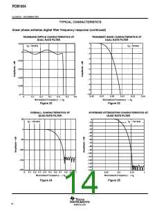
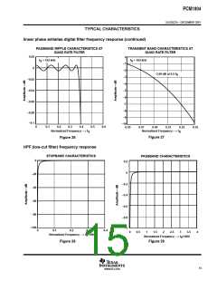
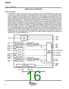
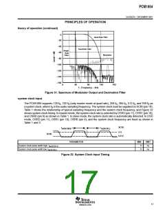
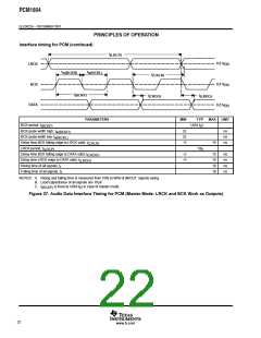
PRINCIPLES OF OPERATION
power-on and reset functions
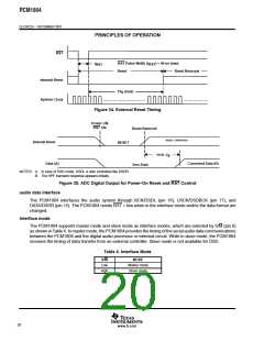
The PCM1804 has both an internal power-on reset circuit and an RST (pin 19). For internal power-on reset,
initialize (reset) is done automatically at the timing the power supply V exceeds 2 V (typ) and V exceeds
DD
CC
4 V (typ). RST accepts external forced reset, and a low level on RST initiates the reset sequence. As the internal
pull-down resistor terminates RST, no connection of RST is equal to the low-level input. As the system clock
is used as a clock signal of the reset circuit, the system clock has to be supplied as soon as power is supplied;
morespecifically, at least three system clocks are required prior to V > 2 V, V
> 4 V and RST = high. During
DD
CC
either V
< 2 V (typ), V
< 4 V (typ), or RST = low, and 1/f (max) count after V
> 2 V (typ),
DD
CC
S
DD
V
> 4 V (typ) and RST = high, the PCM1804 stays in the reset state and the digital output is forced to zero.
CC
The digital output is valid after the reset state is released and the time of 1116/f is passed. Figure 33 and
S
Figure 34 illustrate the internal power on reset and external reset timing. Figure 35 illustrates the digital output
for power on reset and control. The PCM1804 needs RST = low when SCKI, LRCK, BCK (in slave mode), and
control pins are changed.
power-down function
The PCM1804 has a power-down feature that is controlled by the RST (pin 19). Entering the power-down mode
is done by keeping the RST low-level input for over 65536/f . In the master mode, the SCKI (pin 18) is used
S
as the clock signal of the power-down counter. While in the slave mode, the SCKI (pin 18) and the LRCK (pin 17)
areusedastheclocksignal. Theclock(s)hastobesupplieduntilthepower-downsequencecompletes. Assoon
as RST goes high, the PCM1804 starts the reset-release sequence described in the power-on and reset
functions section.
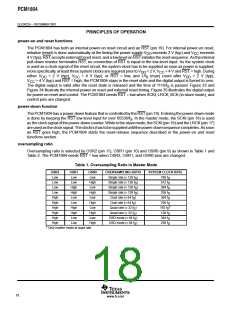
oversampling ratio
Oversampling ratio is selected by OSR2 (pin 11), OSR1 (pin 10) and OSR0 (pin 9) as shown in Table 1 and
Table 2. The PCM1804 needs RST = low when OSR2, OSR1, and OSR0 pins are changed.
Table 1. Oversampling Ratio in Master Mode
OSR2
Low
OSR1
Low
Low
High
High
Low
Low
High
High
Low
Low
OSR0
Low
High
Low
High
Low
High
Low
High
Low
High
OVERSAMPLING RATIO
Single rate (× 128 f )
SYSTEM CLOCK RATE
768 f
512 f
384 f
256 f
384 f
256 f
S
S
S
S
S
S
S
Low
Single rate (× 128 f )
S
Low
Single rate (× 128 f )
S
Low
Single rate (× 128 f )
S
High
High
High
High
High
High
Dual rate (× 64 f )
S
Dual rate (× 64 f )
S
{
S
S
S
Quad rate (× 32 f )
192 f
S
S
Quad rate (× 32 f )
128 f
384 f
256 f
S
DSD mode (× 64 f )
S
DSD mode (× 64 f )
S
†
Only master mode at quad rate
18
www.ti.com

 BB [ BURR-BROWN CORPORATION ]