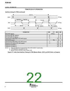
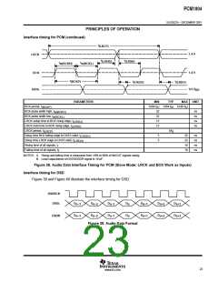
PCM1804
SLES022A – DECEMBER 2001
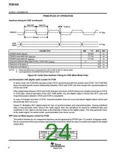
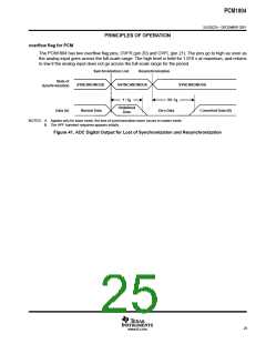
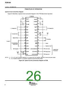
PRINCIPLES OF OPERATION
typical circuit connection diagram
Figure 42 illustrates a typical circuit connection diagram in the PCM data format operation.
PCM1804
C
C
1
2
+
+
28 +
1
2
V
L
REF
V
R
REF
27
26
25
24
23
AGNDL
AGNDR
C
C
4
3
3
4
+
V
V
V
L
V
COM
R
COM
L+
IN
V
V
R+
+
+
IN
L-Channel In
Format [1:0]
R-Channel In
5
6
L–
–
IN
–
R–
IN
FMT0
FMT1
AGND
5 V
C
6
7
8
9
22
21
20
19
18
17
+
V
CC
Master/Slave
S/M
OVFL
Overflow
OSR0
OSR1
OSR2
OVFR
RST
Control
10
11
12
13
Oversampling
Ratio [2:0]
Reset
System Clock
SCKI
BYPAS
DGND
LRCK/DSDBCK
BCK/DSDL
HPF Bypass
3.3 V
L/R Clock
Data Clock
Data Out
Audio Data
Processor
16
15
C
5
+14
V
DD
DATA/DSDR
NOTES: A. C1, C2, C5, and C6: Bypass capacitor 0.1-µF ceramic and 10-µF tantalum, depends on layout and power supply.
B. C3, C4: Bypass capacitor 0.1-µF tantalum, depends on layout and power supply.
Figure 42. Typical Circuit Connection Diagram at PCM
26
www.ti.com

 BB [ BURR-BROWN CORPORATION ]