PCM1804
SLES022A – DECEMBER 2001
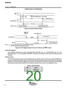
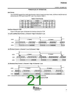
PRINCIPLES OF OPERATION
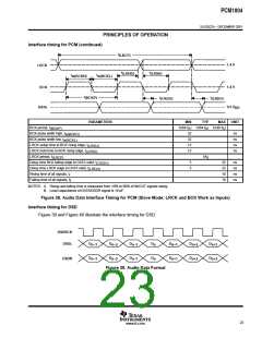
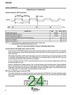
interface timing for DSD (continued)
t
t
w(BCKL)
w(BCKH)
t
(CKDO)
DSDBCK
0.5 V
0.5 V
DD
DD
t
(BCKP)
DSDL
DSDR
PARAMETERS
MIN
TYP
354.308
177.154
177.154
MAX
UNIT
ns
DSDBCK period, t
(BCKP)
DSDBCK pulse width high, t
ns
w(BCKH)
DSDBCK pulse width low, t
ns
w(BCKL)
Delay time DSDBCK falling edge to DSDL, DSDR valid, t
(CKDO)
–5
15
10
10
ns
Rising time of all signals, t
ns
r
Falling time of all signals, t
ns
f
NOTES: A. Rising and falling time is measured from 10% to 90% of IN/OUT signals swing.
B. Load capacitance of DSDBCK/DSDL/DSDR signal is 10 pF.
Figure 40. Audio Data Interface Timing for DSD (Mast Mode Only)
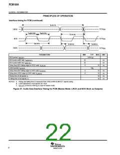
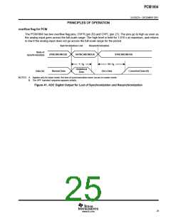
synchronization with digital audio system for PCM
In slave mode, the PCM1804 operates under LRCK synchronized with the system clock SCKI. The PCM1804
does not need specific phase relationship between LRCK and SCKI, but does require the synchronization of
LRCK and SCKI.
If the relationship between LRCK and SCKI changes more than ±6 BCK during one sample period due to LRCK
or SCKI jitter, internal operation of the ADC halts within 1/f and digital output is forced into BPZ code until
S
resynchronization between LRCK and SCKI is completed.
In case of changes less than ±5 BCK, resynchronization does not occur and above digital output control and
discontinuity does not occur.
Figure 41 illustrates ADC digital output for loss of synchronization and resynchronization. During undefined
data, it may generate some noise in the audio signal. Also, the transitions of normal to undefined data and
undefined or zero data to normal make a discontinuity of data on the digital output. This may generate noise
in the audio signal. In master mode, synchronization loss never occurs.
HPF (low-cut filter) bypass control for PCM
The built-in function for dc component rejection can be bypassed by BYPAS (pin 12) control. In bypass mode,
the dc component of the input analog signal and the internal dc offset are also converted and output in the digital
output data.
Table 6. HPF Bypass Control
BYPASS
Low
LPF (HIGH-PASS FILTER) MODE
Normal (dc cut) mode
High
Bypass (through) mode
24
www.ti.com

 BB [ BURR-BROWN CORPORATION ]