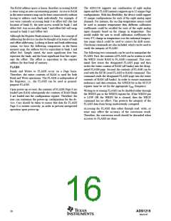
DETAILED REGISTER DEFINITIONS
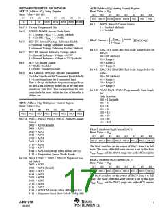
SETUP (Address 00H) Setup Register
Reset Value = iii01110
ACR (Address 02H) Analog Control Register
Reset Value = 00H
bit 7
bit 6
bit 5
bit 4
bit 3
bit 2
bit 1
bit 0
bit 7
bit 6
bit 5
bit 4
bit 3
bit 2
bit 1
bit 0
BOCS
IDAC2R1 IDAC2R0 IDAC1R1 IDAC1R0
PGA2
PGA1
PGA0
ID
ID
ID
SPEED
REF EN
REF HI
BUF EN BIT ORDER
bit 7
BOCS: Burnout Current Source
0 = Disabled (default)
1 = Enabled
bit 7-5 Factory Programmed Bits
bit 4
bit 3
bit 2
bit 1
bit 0
SPEED: FLASH Access Clock Speed
0 : 2.30MHz > fOSC > 3.12MHz (default)
1 : 3.12MHz > fOSC > 4.13MHz
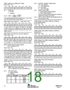
VREF
2RANGE−1 DAC Code
IDAC Current =
(
)
)
(
REF EN: Internal Voltage Reference Enable
0 = Internal Voltage Reference Disabled
1 = Internal Voltage Reference Enabled (default)
8• RDAC
bit 6-5 IDAC2R1: IDAC2R0: Full-Scale Range Select for
REF HI: Internal Reference Voltage Select
0 = Internal Reference Voltage = 1.25V
1 = Internal Reference Voltage = 2.5V (default)
IDAC2
00 = Off (default)
01 = Range 1
10 = Range 2
11 = Range 3
BUF EN: Buffer Enable
0 = Buffer Disabled
1 = Buffer Enabled (default)
bit 4-3 IDAC1R1: IDAC1R0: Full-Scale Range Select for
BIT ORDER: Set Order Bits are Transmitted
0 = Most Significant Bit Transmitted First (default)
1 = Least Significant Bit Transmitted First
Data is always shifted into the part most significant
bit first. Data is always shifted out of the part most
significant byte first. This configuration bit only
controls the bit order within the byte of data that is
shifted out.
IDAC1
00 = Off (default)
01 = Range 1
10 = Range 2
11 = Range 3
bit 2-0 PGA2: PGA1: PGA0: Programmable Gain Ampli-
fier
Gain Selection
000 = 1 (default)
001 = 2
MUX (Address 01H) Multiplexer Control Register
Reset Value = 01H
010 = 4
011 = 8
bit 7
bit 6
bit 5
bit 4
bit 3
bit 2
bit 1
bit 0
100 = 16
101 = 32
110 = 64
111 = 128
PSEL3
PSEL2
PSEL1
PSEL0
NSEL3
NSEL2
NSEL1
NSEL0
bit 7-4 PSEL3: PSEL2: PSEL1: PSEL0: Positive Channel
Select
0000 = AIN0 (default)
0001 = AIN1
0010 = AIN2
IDAC1 (Address 03H) Current DAC 1
Reset Value = 00H
0011 = AIN3
bit 7
bit 6
bit 5
bit 4
bit 3
bit 2
bit 1
bit 0
0100 = AIN4
0101 = AIN5
IDAC1_7 IDAC1_6 IDAC1_5 IDAC1_4 IDAC1_3 IDAC1_2 IDAC1_1 IDAC1_0
0110 = AIN6
0111 = AIN7
1xxx = AINCOM (except when all bits are 1’s)
1111 = Temperature Sensor Diode Anode
The DAC code bits set the output of DAC1 from 0 to full-
scale. The value of the full-scale current is set by this Byte,
VREF, RDAC, and the DAC1 range bits in the ACR register.
bit 3-0 NSEL3: NSEL2: NSEL1: NSEL0: Negative Chan-
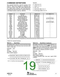
IDAC2 (Address 04H) Current DAC 2
Reset Value = 00H
nel Select
0000 = AIN0
0001 = AIN1 (default)
0010 = AIN2
bit 7
bit 6
bit 5
bit 4
bit 3
bit 2
bit 1
bit 0
IDAC2_7 IDAC2_6 IDAC2_5 IDAC2_4 IDAC1_3 IDAC1_2 IDAC1_1 IDAC1_0
0011 = AIN3
0100 = AIN4
0101 = AIN5
0110 = AIN6
The DAC code bits set the output of DAC2 from 0 to full-
scale. The value of the full-scale current is set by this Byte,
VREF, RDAC, and the DAC2 range bits in the ACR register.
0111 = AIN7
1xxx = AINCOM (except when all bits are 1’s)
1111 = Temperature Sensor Diode Cathode Analog GND
ADS1218
17
SBAS187

 BB [ BURR-BROWN CORPORATION ]