Operands:
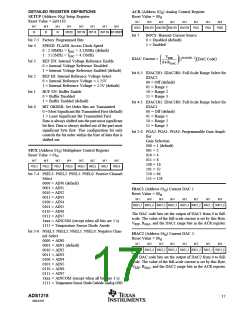
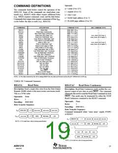
COMMAND DEFINITIONS
n = count (0 to 127)
r = register (0 to 15)
x = don’t care
The commands listed below control the operation of the
ADS1218. Some of the commands are stand-alone com-
mands (e.g., RESET) while others require additional bytes
(e.g., WREG requires command, count, and the data bytes).
Commands that output data require a minimum of four fOSC
cycles before the data is ready (e.g., RDATA).
a = RAM bank address (0 to 7)
f = FLASH page address (0 to 31)
COMMANDS
DESCRIPTION
COMMAND BYTE
2ND COMMAND BYTE
RDATA
RDATAC
STOPC
RREG
RRAM
CREG
CREGA
WREG
WRAM
RF2R
WR2F
Read Data
0000 0001 (01H)
0000 0011 (03H)
0000 1111 (0FH)
0001 r r r r (1xH)
0010 0aaa (2xH)
0100 0aaa (4xH)
0100 1000 (48H)
0101 r r r r (5xH)
0110 0aaa (6xH)
100f f f f f (8, 9xH)
101f f f f f (A,BxH)
1100 0aaa (CxH)
1101 0aaa (DxH)
1101 1000 (D8H)
1101 1111 (DFH)
1110 0aaa (ExH)
1110 1000 (E8H)
1110 1100 (ECH)
1111 0000 (F0H)
1111 0001 (F1H)
1111 0010 (F2H)
1111 0011 (F3H)
1111 0100 (F4H)
1111 1100 (FCH)
1111 1101 (FDH)
1111 1110 (FEH)
—
—
—
Read Data Continuously
Stop Read Data Continuously
Read from REG Bank “rrrr”
Read from RAM Bank “aaa”
Copy REGs to RAM Bank “aaa”
Copy REGS to all RAM Banks
Write to REG “rrrr”
Write to RAM Bank “aaa”
Read FLASH page to RAM
Write RAM to FLASH page
Copy RAM Bank “aaa” to REG
Calc RAM Bank “aaa” Checksum
Calc all RAM Bank Checksum
Calc REG Checksum
xxxx_nnnn (# of reg-1)
xnnn_nnnn (# of bytes-1)
—
—
xxxx_nnnn (# of reg-1)
xnnn_nnnn (# of bytes-1)
—
—
—
—
—
—
—
—
—
—
—
—
—
—
—
—
—
CRAM
CSRAMX
CSARAMX
CSREG
CSRAM
CSARAM
CSFL
SELFCAL
SELFOCAL
SELFGCAL
SYSOCAL
SYSGCAL
DSYNC
SLEEP
Calc RAM Bank “aaa” Checksum
Calc all RAM Banks Checksum
Calc FLASH Checksum
Self Cal Offset and Gain
Self Cal Offset
Self Cal Gain
Sys Cal Offset
Sys Cal Gain
Sync DRDY
Put in SLEEP Mode
Reset to Power-Up Values
RESET
NOTE: (1) The data received by the A/D is always MSB First, the data out format is set by the BIT ORDER bit in ACR reg.
TABLE III. Command Summary.
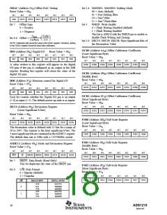
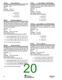
RDATA
Read Data
RDATAC
Read Data Continuous
Description: Read a single data value from the Data Output
Register (DOR) which is the most recent conversion result.
This is a 24-bit value.
Description: Read Data Continuous mode enables the con-
tinuous output of new data on each DRDY. This command
eliminates the need to send the Read Data Command on each
DRDY. This mode may be terminated by either the STOP
Read Continuous command or the RESET command.
Operands: None
Bytes:
1
Operands: None
Encoding: 0000 0001
Bytes:
1
Data Transfer Sequence:
Encoding: 0000 0011
Data Transfer Sequence:
Command terminated when “uuuu uuuu” equals STOPC
or RESET.
0000 0001
xxxx xxxx
• • •(1)
xxxx xxxx
MSB
xxxx xxxx
Mid-Byte
xxxx xxxx
LSB
DIN
• • •(1)
DOUT
DIN
0000 0011
• • •(1)
uuuu uuuu
MSB
uuuu uuuu
Mid-Byte
uuuu uuuu
LSB
NOTE: (1) For wait time, refer to timing specification.
• • •
DOUT
DRDY
DIN
xxxx xxxx
• • •(1)
• • •
xxxx
MSB
xxxx
xxxx
• • •
DOUT
Mid-Byte
LSB
NOTE: (1) For wait time, refer to timing specification.
ADS1218
19
SBAS187

 BB [ BURR-BROWN CORPORATION ]