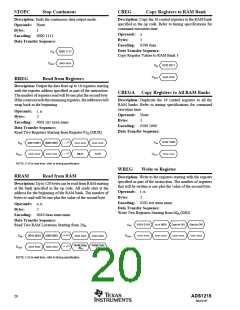
WRAM
Write to RAM
CRAM
Copy RAM Bank to Registers
Description: Write up to 128 RAM locations starting at the
beginning of the RAM bank specified as part of the instruc-
tion. ThenumberofbyteswrittenisRAMisoneplusthevalue
of the second byte.
Description: Copy the selected RAM Bank to the Configura-
tion Registers. This will overwrite all of the registers with the
data from the RAM bank.
Operands:
Bytes:
a
Operands: a, n
1
Bytes:
2
Encoding: 1100 0aaa
Encoding: 0110 0aaa xnnn nnnn
Data Transfer Sequence:
Data Transfer Sequence:
Copy RAM Bank 0 to the Registers
Write to Two RAM Locations starting from 10H
1100 0000
xxxx xxxx
DIN
Data for
10H
Data for
DIN
0110 0001
xxxx xxxx
x000 0001
xxxx xxxx
11H
DOUT
DOUT
xxxx xxxx
xxxx xxxx
CSRAMX
Calculate RAM Bank Checksum
RF2R Read FLASH Page to RAM
Description: Calculate the checksum of the selected RAM
Bank. The checksum is calculated as a sum of all the bytes
with the carry ignored. The ID, DRDY and DIO bits are
masked so they are not included in the checksum.
Description: Read the selected FLASH page to the RAM.
Operands:
Bytes:
f
1
Operands:
Bytes:
a
Encoding: 100f ffff
1
Data Transfer Sequence:
Encoding: 1101 0aaa
Read FLASH Page 2 to RAM
Data Transfer Sequence:
Calculate Checksum for RAM Bank 3
1000 0010
DIN
1101 0011
xxxx xxxx
DIN
xxxx xxxx
DOUT
DOUT
WR2F Write RAM to FLASH
Description: Write the contents of RAM to the selected
FLASH page.
CSARAMX Calculate the Checksum
for all RAM Banks
Operands:
Bytes:
f
Description: Calculate the checksum of all RAM Banks. The
checksum is calculated as a sum of all the bytes with the carry
ignored. The ID, DRDY and DIO bits are masked so they are
not included in the checksum.
1
Encoding: 101f ffff
Data Transfer Sequence:
Write RAM to FLASH page 31
Operands: None
Bytes:
1
1011 1111
DIN
Encoding: 1101 1000
Data Transfer Sequence:
xxxx xxxx
DOUT
1101 1000
xxxx xxxx
DIN
DOUT
ADS1218
21
SBAS187

 BB [ BURR-BROWN CORPORATION ]