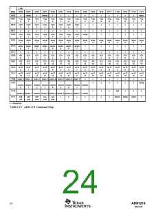
STOPC
Stop Continuous
CREG
Copy Registers to RAM Bank
Description: Ends the continuous data output mode.
Operands: None
Description: Copy the 16 control registers to the RAM bank
specified in the op code. Refer to timing specifications for
command execution time.
Bytes:
1
Operands:
Bytes:
a
Encoding: 0000 1111
1
Data Transfer Sequence:
Encoding: 0100 0aaa
Data Transfer Sequence:
Copy Register Values to RAM Bank 3
0000 1111
xxxx xxxx
DIN
DOUT
0100 0011
xxxx xxxx
DIN
DOUT
RREG
Read from Registers
Description: Output the data from up to 16 registers starting
with the register address specified as part of the instruction.
The number of registers read will be one plus the second byte.
Ifthecountexceedstheremainingregisters,theaddresseswill
wrap back to the beginning.
CREGA Copy Registers to All RAM Banks
Description: Duplicate the 16 control registers to all the
RAM banks. Refer to timing specifications for command
execution time.
Operands: r, n
Operands: None
Bytes:
2
Bytes:
1
Encoding: 0001 rrrr xxxx nnnn
Encoding: 0100 1000
Data Transfer Sequence:
Read Two Registers Starting from Register 01H (MUX)
Data Transfer Sequence:
0100 1000
xxxx xxxx
DIN
0001 0001
xxxx xxxx
0000 0001
xxxx xxxx
• • •(1)
xxxx xxxx
MUX
xxxx xxxx
ACR
DIN
• • •(1)
DOUT
DOUT
NOTE: (1) For wait time, refer to timing specification.
WREG
Write to Register
RRAM
Read from RAM
Description: Write to the registers starting with the register
specified as part of the instruction. The number of registers
that will be written is one plus the value of the second byte.
Description: Up to 128 bytes can be read from RAM starting
at the bank specified in the op code. All reads start at the
address for the beginning of the RAM bank. The number of
bytes to read will be one plus the value of the second byte.
Operands: r, n
Bytes:
2
Encoding: 0101 rrrr xxxx nnnn
Operands: a, n
Data Transfer Sequence:
Write Two Registers Starting from 06H (DIO)
Bytes:
2
Encoding: 0010 0aaa xnnn nnnn
Data Transfer Sequence:
Read Two RAM Locations Starting from 20H
DIN
0101 0110
xxxx xxxx
xxxx 0001
xxxx xxxx
Data for DIO
xxxx xxxx
Data for DIR
xxxx xxxx
0010 0010
xxxx xxxx
x000 0001
xxxx xxxx
• • •(1)
xxxx xxxx
xxxx xxxx
DOUT
DIN
RAM Data
20H
RAM Data
21H
• • •(1)
DOUT
NOTE: (1) For wait time, refer to timing specification.
ADS1218
20
SBAS187

 BB [ BURR-BROWN CORPORATION ]