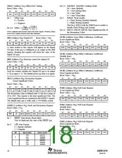
VOLTAGE REFERENCE
DIGITAL I/O INTERFACE
The voltage reference used for the ADS1218 can either be
internal or external. The power-up configuration for the
voltage reference is 2.5V internal. The selection for the
voltage reference is made through the status configuration
register.
The ADS1218 has eight pins dedicated for digital I/O. The
default power-up condition for the digital I/O pins are as
inputs. All of the digital I/O pins are individually configurable
as inputs or outputs. They are configured through the DIR
control register. The DIR register defines whether the pin is an
input or output, and the DIO register defines the state of the
digital output. When the digital I/O are configured as inputs,
DIO is used to read the state of the pin.
The internal voltage reference is selectable as either 1.25V
or 2.5V (AVDD = 5V only). The VREFOUT pin should have a
0.1µF capacitor to AGND.
The external voltage reference is differential and is repre-
sented by the voltage difference between the pins: +VREF
and –VREF. The absolute voltage on either pin (+VREF and
–VREF) can range from AGND to AVDD, however, the
differential voltage must not exceed 2.5V. The differential
voltage reference provides easy means of performing
ratiometric measurement.
SERIAL INTERFACE
The serial interface is standard four-wire SPI compatible (DIN,
DOUT, SCLK, and CS). The ADS1218 also offers the flexibil-
ity to select the polarity of the serial clock through the POL
pin. The serial interface can be clocked up to fOSC/4. If CS
goes HIGH, the serial interface is reset. When CS goes LOW,
a new command is expected.
VRCAP PIN
The serial interface operates independently of DRDY. DRDY
is used to indicate availability of data in the DOR. In order to
ensure the validity of the data being read, DOR timing
requirements must be met.
This pin provides a bypass cap for noise filtering on internal
VREF circuitry only. The recommended capacitor is a 0.001µF
ceramic cap. If an external VREF is used, this pin can be left
unconnected.
DSYNC OPERATION
CLOCK GENERATOR
DSYNC is used to provide for synchronization of the A/D
conversion with an external event. Synchronization can be
achieved either through the DSYNC pin or the DSYNC
command. When the DSYNC pin is used, the filter counter
is reset on the falling edge of DSYNC. The modulator is held
in reset until DSYNC is taken HIGH. Synchronization
occurs on the next rising edge of the system clock after
DSYNC is taken HIGH.
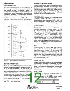
The clock source for the ADS1218 can be provided from a
crystal, ceramic resonator, oscillator, or external clock. When
the clock source is a crystal or ceramic resonator, external
capacitors must be provided to ensure start-up and a stable
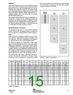
clock frequency. This is shown in Figure 4 and Table I.
When the DSYNC command is sent, the filter counter is
reset after the last SCLK on the DSYNC command. The
modulator is held in RESET until the next edge of SCLK is
detected. Synchronization occurs on the next rising edge of
the system clock after the first SCLK after the DSYNC
command.
XIN
C1
C2
Crystal
or
Ceramic Resonator
XOUT
POWER-UP—SUPPLY VOLTAGE RAMP RATE
The power-on reset circuitry was designed to accommodate
digital supply ramp rates as slow as 1V/10ms. To ensure
proper operation, the power supply should ramp monotoni-
cally. The POR issues the RESET command as described
below.
FIGURE 4. Crystal or Ceramic Resonator Connection.
CLOCK
PART
SOURCE FREQUENCY
C1
C2
NUMBER
Crystal
Crystal
Crystal
Crystal
2.4576
4.9152
4.9152
4.9152
0-20pF 0-20pF ECS, ECSD 2.45 - 32
RESET
0-20pF 0-20pF
0-20pF 0-20pF
ECS, ECSL 4.91
ECS, ECSD 4.91
There are three methods of reset. The RESET pin, the
RESET command, and the SCLK Reset pattern. They all
perform the same function. After a reset, the FLASH data
values from Page 0 are loaded into RAM, subsequently data
values from Bank 0 of RAM are loaded into the configura-
tion registers.
0-20pF 0-20pF CTS, MP 042 4M9182
TABLE I. Typical Clock Sources.
ADS1218
14
SBAS187

 BB [ BURR-BROWN CORPORATION ]