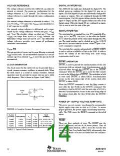
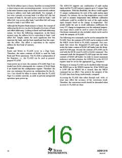
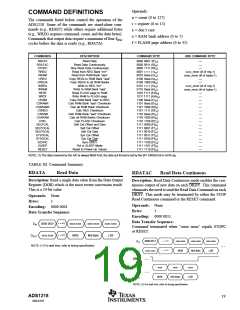
MEMORY
basis. Also, the RAM can be directly read or written through
the serial interface on power-up. The banks allow separate
storage of settings for each input.
Three types of memory are used on the ADS1218: registers,
RAM, and FLASH. 16 registers directly control the various
functions (PGA, DAC value, Decimation Ratio, etc.) and can
be directly read or written to. Collectively, the registers contain
all the information needed to configure the part, such as data
format, mux settings, calibration settings, decimation ratio, etc.
Additional registers, such as conversion data, are accessed
through dedicated instructions.
Configuration
Register Bank
16 bytes
RAM
128 Bytes
FLASH
4k Bytes
SETUP
MUX
ACR
IDAC1
IDAC2
ODAC
DIO
The on-chip FLASH can be used to store non-volatile data. The
FLASH data is separate from the configuration registers and
therefore can be used for any purpose, in addition to device
configuration. The FLASH page data is read and written in 128
byte blocks through the RAM banks, i.e. all RAM banks map
to a single page of FLASH, as shown in Figure 5.
DIR
Bank 0
DEC0
M/DEC1
OCR0
OCR1
OCR2
FSR0
FSR1
FSR2
16 bytes
Bank 2
16 bytes
REGISTER BANK TOPOLOGY
Page 0
128 bytes
The operation of the device is set up through individual
registers. The set of the 16 registers required to configure the
device is referred to as a Register Bank, as shown in Figure 5.
RAM
Reads and Writes to Registers and RAM occur on a byte
basis. However, copies between registers and RAM occurs
on a bank basis. The RAM is independent of the Registers,
i.e.: the RAM can be used as general-purpose RAM.
Bank 7
16 bytes
The ADS1218 supports any combination of eight analog
inputs. With this flexibility, the device could easily support
eight unique configurations—one per input channel. In order
to facilitate this type of usage, eight separate register banks are
available. Therefore, each configuration could be written once
and recalled as needed without having to serially retransmit all
the configuration data. Checksum commands are also in-
cluded, which can be used to verify the integrity of RAM.
Page 31
128 bytes
The RAM provides eight “banks”, with a bank consisting of
16 bytes. The total size of the RAM is 128 bytes. Copies
between the registers and RAM are performed on a bank
FIGURE 5. Memory Organization.
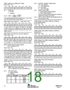
ADDRESS
REGISTER
BIT 7
BIT 6
BIT 5
BIT 4
BIT 3
BIT 2
BIT 1
BIT 0
00H
01H
02H
03H
04H
05H
06H
07H
08H
09H
0AH
0BH
0CH
0DH
0EH
0FH
SETUP
MUX
ID
ID
ID
SPEED
PSEL0
REF EN
NSEL3
IDAC1R0
IDAC1_3
IDAC2_3
OSET_3
DIO_3
REF HI
NSEL2
PGA2
BUF EN
NSEL1
PGA1
BIT ORDER
NSEL0
PGA0
PSEL3
BOCS
PSEL2
IDAC2R1
IDAC1_6
IDAC2_6
OSET_6
DIO_6
PSEL1
IDAC2R0
IDAC1_5
IDAC2_5
OSET_5
DIO_5
ACR
IDAC1R1
IDAC1_4
IDAC2_4
OSET_4
DIO_4
IDAC1
IDAC2
ODAC
DIO
IDAC1_7
IDAC2_7
SIGN
IDAC1_2
IDAC2_2
OSET_2
DIO_2
IDAC1_1
IDAC2_1
OSET_1
DIO_1
IDAC1_0
IDAC2_0
OSET_0
DIO_0
DIO_7
DIR_7
DIR
DIR_6
DIR_5
DIR_4
DIR_3
DIR_2
DIR_1
DIR_0
DEC0
M/DEC1
OCR0
OCR1
OCR2
FSR0
FSR1
FSR2
DEC07
DRDY
DEC06
U/B
DEC05
SMODE1
OCR05
OCR13
OCR21
FSR05
FSR13
FSR21
DEC04
SMODE0
OCR04
OCR12
OCR20
FSR04
DEC03
WREN
DEC02
DEC10
OCR02
OCR10
OCR18
FSR02
FSR10
FSR18
DEC01
DEC09
OCR01
OCR09
OCR17
FSR01
FSR09
FSR17
DEC00
DEC08
OCR00
OCR08
OCR16
FSR00
OCR07
OCR15
OCR23
FSR07
FSR15
FSR23
OCR06
OCR14
OCR22
FSR06
FSR14
FSR22
OCR03
OCR11
OCR19
FSR03
FSR11
FSR19
FSR12
FSR08
FSR20
FSR16
TABLE II. Registers.
ADS1218
15
SBAS187

 BB [ BURR-BROWN CORPORATION ]