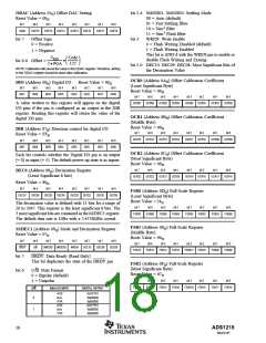
ODAC (Address 05H) Offset DAC Setting
Reset Value = 00H
bit 5-4 SMODE1: SMODE0: Settling Mode
00 = Auto (default)
01 = Fast Settling filter
bit 7
bit 6
bit 5
bit 4
bit 3
bit 2
bit 1
bit 0
10 = Sinc2 filter
SIGN
OSET6
OSET5
OSET4
OSET3
OSET2
OSET1
OSET0
11 = Sinc3 Flash filter
bit 7
Offset Sign
0 = Positive
bit 3
WREN: Write Enable
0 = Flash Writing Disabled (default)
1 = Flash Writing Enabled
This bit is AND’d with the WREN pin to enable or
disable Flash Writing and Erasing
1 = Negative
VREF
Code
127
•
bit 6-0 Offset =
2 • PGA
bit 2-0 DEC10: DEC09: DEC08: Most Significant Bits of
the Decimation Value
NOTE: Calibration will cancel the value in the ODAC register. Therefore, writing
to the ODAC register should be done after calibration.
OCR0 (Address 0AH) Offset Calibration Coefficient
(Least Significant Byte)
DIO (Address 06H) Digital I/O
Reset Value = 00H
bit 7
bit 6
bit 5
bit 4
bit 3
bit 2
bit 1
bit 0
Reset Value = 00H
DIO7
DIO6
DIO5
DIO4
DIO3
DIO2
DIO1
DIO0
bit 7
bit 6
bit 5
bit 4
bit 3
bit 2
bit 1
bit 0
A value written to this register will appear on the digital
I/O pins if the pin is configured as an output in the DIR
register. Reading this register will return the value of the
digital I/O pins.
OCR07
OCR06
OCR05
OCR04
OCR03
OCR02
OCR01
OCR00
OCR1 (Address 0BH) Offset Calibration Coefficient
(Middle Byte)
Reset Value = 00H
DIR (Address 07H) Direction control for digital I/O
Reset Value = FFH
bit 7
bit 6
bit 5
bit 4
bit 3
bit 2
bit 1
bit 0
OCR15
OCR14
OCR13
OCR12
OCR11
OCR10
OCR09
OCR08
bit 7
bit 6
bit 5
bit 4
bit 3
bit 2
bit 1
bit 0
DIR7
DIR6
DIR5
DIR4
DIR3
DIR2
DIR1
DIR0
OCR2 (Address 0CH) Offset Calibration Coefficient
(Most Significant Byte)
Reset Value = 00H
Each bit controls whether the Digital I/O pin is an output
(= 0) or input (= 1). The default power-up state is as inputs.
bit 7
bit 6
bit 5
bit 4
bit 3
bit 2
bit 1
bit 0
DEC0 (Address 08H) Decimation Register
(Least Significant 8 bits)
OCR23
OCR22
OCR21
OCR20
OCR19
OCR18
OCR17
OCR16
Reset Value = 80H
bit 7
bit 6
bit 5
bit 4
bit 3
bit 2
bit 1
bit 0
FSR0 (Address 0DH) Full-Scale Register
(Least Significant Byte)
DEC07
DEC06
DEC05
DEC04
DEC03
DEC02
DEC01
DEC00
Reset Value = 24H
The decimation value is defined with 11 bits for a range of
20 to 2047. This register is the least significant 8 bits. The
3 most significant bits are contained in the M/DEC1 register.
The default data rate is 10Hz with a 2.4576MHz crystal.
bit 7
bit 6
bit 5
bit 4
bit 3
bit 2
bit 1
bit 0
FSR07
FSR06
FSR05
FSR04
FSR03
FSR02
FSR01
FSR00
FSR1 (Address 0EH) Full-Scale Register
(Middle Byte)
Reset Value = 90H
M/DEC1 (Address 09H) Mode and Decimation Register
Reset Value = 07H
bit 7
bit 6
bit 5
bit 4
bit 3
bit 2
bit 1
bit 0
bit 7
bit 6
bit 5
bit 4
bit 3
bit 2
bit 1
bit 0
DRDY
U/B
SMODE1 SMODE0
WREN
DEC10
DEC09
DEC08
FSR15
FSR14
FSR13
FSR12
FSR011
FSR10
FSR09
FSR08
bit 7
DRDY: Data Ready (Read Only)
This bit duplicates the state of the DRDY pin.
FSR2 (Address 0FH) Full-Scale Register
(Most Significant Byte)
Reset Value = 67H
bit 6
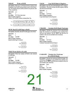
U/B: Data Format
0 = Bipolar (default)
1 = Unipolar
bit 7
bit 6
bit 5
bit 4
bit 3
bit 2
bit 1
bit 0
FSR23
FSR22
FSR21
FSR20
FSR019
FSR18
FSR17
FSR16
U/B
ANALOG INPUT
DIGITAL OUTPUT
+FSR
Zero
–FSR
+FSR
Zero
0x7FFFFF
0x000000
0x800000
0xFFFFFF
0x000000
0x000000
0
1
–FSR
ADS1218
18
SBAS187

 BB [ BURR-BROWN CORPORATION ]