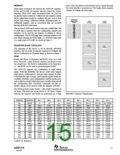
The RAM address space is linear, therefore accessing RAM
is done using an auto-incrementing pointer. Access to RAM
in the entire memory map can be done consecutively without
having to address each bank individually. For example, if
you were currently accessing bank 0 at offset 0xF (the last
location of bank 0), the next access would be bank 1 and
offset 0x0. Any access after bank 7 and offset 0xF will wrap
around to bank 0 and Offset 0x0.
The ADS1218 supports any combination of eight analog
inputs and the FLASH memory supports up to 32 unique Page
configurations. With this flexibility, the device could support
32 unique configurations for each of the eight analog input
channels. For instance, the on-chip temperature sensor could
be used to monitor temperature then different calibration
coefficients could be recalled for each of the eight analog
input channels based on the change in temperature. This
would enable the user to recall calibration coefficients for
every 4°C change in temperature over the industrial tempera-
ture range which could be used to correct for drift errors.
Checksum commands are also included, which can be used to
verify the integrity of FLASH.
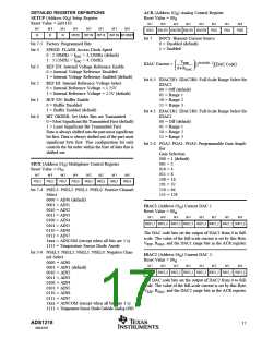
Although the Register Bank memory is linear, the concept of
addressing the device can also be thought of in terms of bank
and offset addressing. Looking at linear and bank addressing
syntax, we have the following comparison: in the linear
memory map, the address 0x14 is equivalent to bank 1 and
offset 0x4. Simply stated, the most significant four bits
represent the bank, and the least significant four bits repre-
sent the offset. The offset is equivalent to the register
address for that bank of memory.
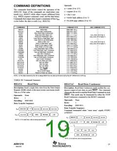
The following two commands can be used to manipulate the
FLASH. First, the contents of FLASH can be written to with
the WR2F (write RAM to FLASH) command. This com-
mand first erases the designated FLASH page and then
writes the entire content of RAM (all banks) into the desig-
nated FLASH page. Second, the contents of FLASH can be
read with the RF2R (read FLASH to RAM) command. This
command reads the designated FLASH page into the entire
contents of RAM (all banks). In order to ensure maximum
endurance and data retention, the SPEED bit in the SETUP
register must be set for the appropriate fOSC frequency.
FLASH
Reads and Writes to FLASH occur on a Page basis.
Therefore, the entire contents of RAM is used for both
Read and Write operations. The FLASH is independent of
the Registers, i.e., the FLASH can be used as general-
purpose FLASH.
Upon power-up or reset, the contents of FLASH Page 0 are
loaded into RAM subsequently the contents of RAM Bank
0 are loaded into the configuration register. Therefore, the
user can customize the power-up configuration for the de-
vice. Care should be taken to ensure that data for FLASH
Page 0 is written correctly, in order to prevent unexpected
operation upon power-up.
Writing to or erasing FLASH can be disabled either through
the WREN pin or the WREN register bit. If the WREN pin
is LOW OR the WREN bit is cleared, then the WR2F
command has no effect. This protects the integrity of the
FLASH data from being inadvertently corrupted.
Accessing the FLASH data either through read, write, or
erase may effect the accuracy of the conversion result.
Therefore, the conversion result should be discarded when
accesses to FLASH are done.
ADS1218
16
SBAS187

 BB [ BURR-BROWN CORPORATION ]