BURNOUT CURRENT SOURCES
OVERVIEW
When the Burnout bit is set in the ACR configuration register,
two current sources are enabled. The current source on the
positive input channel sources approximately 2µA of current.
The current source on the negative input channel sinks ap-
proximately 2µA. This allows for the detection of an open
circuit (full-scale reading) or short circuit (0V differential
reading) on the selected input differential pair.
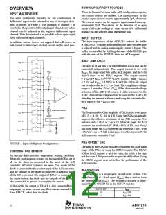
INPUT MULTIPLEXER
The input multiplexer provides for any combination of
differential inputs to be selected on any of the input chan-
nels, as shown in Figure 1. For example, if channel 1 is
selected as the positive differential input channel, any other
channel can be selected as the negative differential input
channel. With this method, it is possible to have up to eight
fully differential input channels.
INPUT BUFFER
The input impedance of the ADS1218 without the buffer
is 5MΩ/PGA. With the buffer enabled, the input voltage range
is reduced and the analog power-supply current is higher. The
buffer is controlled by ANDing the state of the BUFEN pin
with the state of the BUFFER bit in the ACR register.
In addition, current sources are supplied that will source or
sink current to detect open or short circuits on the input pins.
IDAC1 AND IDAC2
A
IN0
The ADS1218 has two 8-bit current output DACs that can be
controlled independently. The output current is set with
RDAC, the range select bits in the ACR register, and the 8-bit
digital value in the IDAC register. The output current
= VREF/(8 • RDAC)(2RANGE–1)(DAC CODE). With VREFOUT
= 2.5V and RDAC = 150kΩ to AGND the full-scale output
can be selected to be 0.5, 1, or 2mA. The compliance voltage
range is 0 to within 1V of AVDD. When the internal voltage
reference of the ADS1218 is used, it is the reference for the
IDAC. An external reference may be used for the IDACs by
disabling the internal reference and tying the external refer-
ence input to the VREFOUT pin.
AIN
AIN
AIN
AIN
AIN
AIN
AIN
1
2
3
4
5
6
7
AVDD
Burnout Current Source On
PGA
Burnout Current Source On
The Programmable Gain Amplifier (PGA) can be set to gains
of 1, 2, 4, 8, 16, 32, 64, or 128. Using the PGA can actually
improve the effective resolution of the A/D converter. For
instance, with a PGA of 1 on a 5V full-scale range, the A/D
converter can resolve to 1µV. With a PGA of 128, on a 40mV
full-scale range, the A/D converter can resolve to 75nV. With
a PGA of 1 on a 5V full-scale range, it would require a 26-bit
A/D converter to resolve 75nV.
AGND
IDAC1
AINCOM
PGA OFFSET DAC
FIGURE 1. Input Multiplexer Configuration.
The input to the PGA can be shifted by half the full-scale input
range of the PGA by using the ODAC register. The ODAC
(Offset DAC) register is an 8-bit value; the MSB is the sign
and the seven LSBs provide the magnitude of the offset. Using
the ODAC register does not reduce the performance of the
A/D converter.
TEMPERATURE SENSOR
An on-chip diode provides temperature sensing capability.
When the configuration register for the input MUX is set to
all 1s, the diode is connected to the input of the A/D
converter. All other channels are open. The anode of the
diode is connected to the positive input of the A/D converter,
and the cathode of the diode is connected to negative input
of the A/D converter. The output of IDAC1 is connected to
the anode to bias the diode and the cathode of the diode is
also connected to ground to complete the circuit.
MODULATOR
The modulator is a single-loop second-order system. The
modulator runs at a clock speed (fMOD) that is derived from
the external clock (fOSC). The frequency division is deter-
mined by the SPEED bit in the SETUP register.
In this mode, the output of IDAC1 is also connected to the
output pin, so some current may flow into an external load
from IDAC1, rather than the diode.
SPEED BIT
fMOD
0
1
fOSC/128
f
OSC/ 256
ADS1218
12
SBAS187

 BB [ BURR-BROWN CORPORATION ]