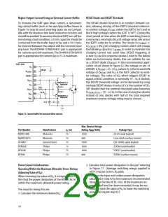
System Considerations
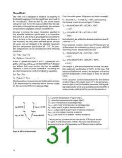
Propagation Delay Difference (PDD)
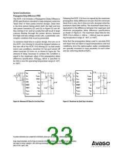
Delaying the HCPL-316J turn-on signals by the maximum
propagation delay difference ensures that the minimum
dead time is zero, but it does not tell a designer what the
maximum dead time will be. The maximum dead time is
equivalent to the difference between the maximum and
minimum propagation delay difference specifications
as shown in Figure 81. The maximum dead time for the
HCPL-316J is 800ns (= 400ns - (-400ns)) over an operat-
ing temperature range of -40°C to 100°C.
The HCPL-316J includes a Propagation Delay Difference
(PDD) specification intended to help designers minimize
“dead time” in their power inverter designs. Dead time
is the time period during which both the high and low
side power transistors (Q1 and Q2 in Figure 62) are off.
Any overlap in Q1 and Q2 conduction will result in large
currents flowing through the power devices between
the high and low voltage motor rails, a potentially cata-
strophic condition that must be prevented.
Note that the propagation delays used to calculate PDD
and dead time are taken at equal temperatures and test
conditions since the optocouplers under consideration
are typically mounted in close proximity to each other
and are switching identical IGBTs.
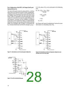
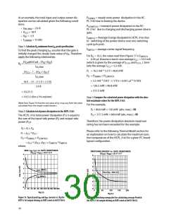
To minimize dead time in a given design, the turn-on of
the HCPL-316J driving Q2 should be delayed (relative to
the turn-off of the HCPL-316J driving Q1) so that under
worst-case conditions, transistor Q1 has just turned off
when transistor Q2 turns on, as shown in Figure 80. The
amount of delay necessary to achieve this condition is
equal to the maximum value of the propagation delay
difference specification, PDD
, which is specified to
MAX
be 400ns over the operating temperature range of -40°C
to 100°C.
I
I
E
E
V
V
V
V
E
V
V
V
V
E
IN+
IN-
IN+
IN-
0.1
µF
0.1
µF
–
+
–
5 V
+
–
5 V
+
V
V
LED2+
LED2+
+
0.1
µF
0.1
µF
–
30 V
30 V
DESAT
DESAT
CC1
CC1
GND1
V
GND1
V
V
CC2
CC2
0.1 µF
0.1 µF
RESET
FAULT
V
RESET
FAULT
V
C
C
+
–
+
–
V
0.1 µF
0.1 µF
OUT
OUT
30 V
30 V
V
V
V
V
LED1+
EE
LED1+
EE
V
V
V
V
LED1-
EE
LED1-
EE
Figure 81. Waveforms for Dead Time Calculation.
Figure 80. Minimum LED Skew for Zero Dead Time.
For product information and a complete list of distributors, please go to our website: www.avagotech.com
Avago, Avago Technologies, and the A logo are trademarks of Avago Technologies in the United States and other countries.
Data subject to change. Copyright © 2005-2009 Avago Technologies. All rights reserved. Obsoletes AV01-0579EN
AV02-0717EN - April 9, 2009

 AVAGO [ AVAGO TECHNOLOGIES LIMITED ]