HCPL-316J
1
2
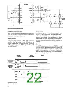
3
4
5
6
7
8
V
V
V
IN+
IN-
HCPL-316J
V
16
15
E
HCPL-316J
V
16
15
E
V
LED2+
100 pF
CC1
+
–
µC
V
LED2+
DESAT 14
3.3
GND1
100 Ω
kΩ
D
DESAT
DESAT 14
V
V
13
12
11
10
9
CC2
RESET
FAULT
V
13
12
11
10
9
CC2
V
C
V
C
OUT
R
g
V
V
LED1+
LED1-
330 pF
V
V
OUT
EE
R
g
V
V
EE
EE
R
PULL-DOWN
V
EE
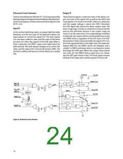
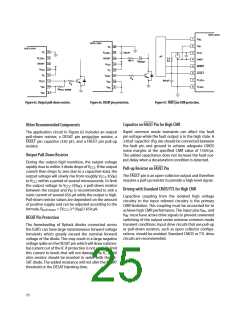
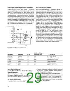
Figure 65. Output pull-down resistor.
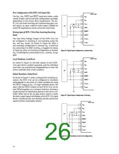
Figure 66. DESAT pin protection.
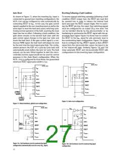
Figure 67. FAULT pin CMR protection.
Capacitor on FAULT Pin for High CMR
Other Recommended Components
Rapid common mode transients can affect the fault
pin voltage while the fault output is in the high state. A
330pF capacitor (Fig. 66) should be connected between
the fault pin and ground to achieve adequate CMOS
noise margins at the specified CMR value of 15kV/µs.
The added capacitance does not increase the fault out-
put delay when a desaturation condition is detected.
The application circuit in Figure 62 includes an output
pull-down resistor, a DESAT pin protection resistor, a
FAULT pin capacitor (330 pF), and a FAULT pin pull-up
resistor.
Output Pull-Down Resistor
During the output high transition, the output voltage
rapidly rises to within 3 diode drops of V . If the output
current then drops to zero due to a capacitive load, the
CC2
Pull-up Resistor on FAULT Pin
The FAULT pin is an open-collector output and therefore
requires a pull-up resistor to provide a high-level signal.
output voltage will slowly rise from roughly V -3(V
)
CC2
BE
to V
within a period of several microseconds. To limit
CC2
the output voltage to V -3(V ), a pull-down resistor
CC2
BE
Driving with Standard CMOS/TTL for High CMR
between the output and V is recommended to sink a
EE
static current of several 650 µA while the output is high.
Pull-down resistor values are dependent on the amount
of positive supply and can be adjusted according to the
Capacitive coupling from the isolated high voltage
circuitry to the input referred circuitry is the primary
CMR limitation. This coupling must be accounted for to
formula, R
= [V -3*(V )]/650 µA.
pull-down
CC2 BE
achieve high CMR performance. The input pins V and
IN+
V
must have active drive signals to prevent unwanted
IN-
DESAT Pin Protection
switching of the output under extreme common mode
transient conditions. Input drive circuits that use pull-up
or pull-down resistors, such as open collector configu-
rations, should be avoided. Standard CMOS or TTL drive
circuits are recommended.
The freewheeling of flyback diodes connected across
the IGBTs can have large instantaneous forward voltage
transients which greatly exceed the nominal forward
voltage of the diode. This may result in a large negative
voltage spike on the DESAT pin which will draw substan-
tial current out of the IC if protection is not used. To limit
this current to levels that will not damage the IC, a 100
ohm resistor should be inserted in series with the DE-
SAT diode. The added resistance will not alter the DESAT
threshold or the DESAT blanking time.
25

 AVAGO [ AVAGO TECHNOLOGIES LIMITED ]