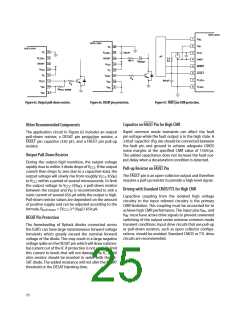
Higher Output Current Using an External Current Buffer:
DESAT Diode and DESAT Threshold
To increase the IGBT gate drive current, a non-invert-
ing current buffer (such as the npn/pnp buffer shown in
Figure 75) may be used. Inverting types are not compat-
ible with the desatura-tion fault protection circuitry and
should be avoided.To preserve the slow IGBT turn-off fea-
ture during a fault condition, a 10 nF capacitor should be
The DESAT diode’s function is to conduct forward cur-
rent, allowing sensing of the IGBT’s saturated collector-
to-emitter voltage, V , (when the IGBT is “on”) and to
CESAT
block high voltages (when the IGBT is “off”). During the
short period of time when the IGBT is switching, there is
commonly a very high dV /dt voltage ramp rate across
CE
connected from the buffer input to V and a 10 W resis-
the IGBT’s collector-to-emitter. This results in I
(=
EE
CHARGE
tor inserted between the output and the common npn/
pnp base. The MJD44H11/MJD45H11 pair is appropriate
for currents up to 8A maximum. The D44VH10/D45VH10
pair is appropriate for currents up to 15 A maximum.
C
x dV /dt) charging current which will charge
D-DESAT CE
the blanking capacitor, C
. In order to minimize this
BLANK
charging current and avoid false DESAT triggering, it
is best to use fast response diodes. Listed in the below
table are fast-recovery diodes that are suitable for use
as a DESAT diode (D
). In the recommended appli-
DESAT
HCPL-316J
cation circuit shown in Figure 62, the voltage on pin 14
(DESAT) is V = V + V , (where V is the forward ON
V
16
15
E
DESAT
F
CE
F
100 pF
V
LED2+
voltage of D
and V is the IGBT collector-to-emit-
DESAT
CE
ter voltage). The value of V which triggers DESAT to
DESAT 14
CE
signal a FAULT condition, is nominally 7V – V . If desired,
F
V
13
12
11
10
9
CC2
this DESAT threshold voltage can be decreased by using
multiple DESAT diodes in series. If n is the number of DE-
SAT diodes then the nominal threshold value becomes
MJD44H11 or
D44VH10
V
C
4.5 Ω
10 Ω
10 nF
V
OUT
2.5 Ω
V
= 7 V – n x V . In the case of using two diodes
CE,FAULT(TH)
F
V
V
EE
EE
instead of one, diodes with half of the total required
maximum reverse-voltage rating may be chosen.
MJD45H11 or
D45VH10
15 V
-5 V
Figure 75. Current buffer for increased drive current.
Max. Reverse Voltage
Part Number
MUR1100E
MURS160T3
UF4007
Manufacturer
Motorola
Motorola
General Semi.
Philips
t
(ns)
Rating, V (Volts)
Package Type
rr
RRM
75
75
75
75
75
75
1000
600
59-04 (axial leaded)
Case 403A (surface mount)
DO-204AL (axial leaded)
SOD64 (axial leaded)
SOD57 (axial leaded)
SOD87 (surface mount)
1000
1000
1000
600
BYM26E
BYV26E
Philips
BYV99
Philips
Power/Layout Considerations
Operating Within the Maximum Allowable Power Ratings
(Adjusting Value of R ):
2. Calculate total power dissipation in the part referring
to Figure 77. (Average switching energy supplied to
HCPL‑316J per cycle vs. R plot);
G
G
3. Compare the input and output power dissipation
calculated in step #2 to the maximum recommended
dissipation for the HCPL-316J. (If the maximum rec-
ommended level has been exceeded, it may be nec-
When choosing the value of R , it is important to con-
G
firm that the power dissipation of the HCPL-316J is
within the maximum allowable power rating.
essary to raise the value of R to lower the switching
power and repeat step #2.)
G
The steps for doing this are:
1. Calculate the minimum desired R ;
G
29

 AVAGO [ AVAGO TECHNOLOGIES LIMITED ]