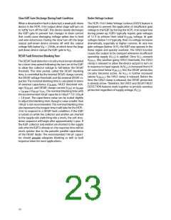
Auto-Reset
Resetting Following a Fault Condition
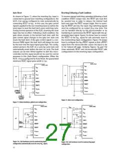
As shown in Figure 72, when the inverting V input is
connected to ground (non-inverting configuration), the
HCPL-316J can be configured to reset automatically by
To resume normal switching operation following a fault
condition (FAULT output low), the RESET pin must first
be asserted low in order to release the internal fault
latch and reset the FAULT output (high). Prior to assert-
IN-
connecting RESET to V . In this case, the gate control
IN+
signal is applied to the non-inverting input as well as the
reset input to reset the fault latch every switching cycle.
During normal operation of the IGBT, asserting the reset
input low has no effect. Following a fault condition, the
gate driver remains in the latched fault state until the
gate control signal changes to the ‘gate low’ state and
resets the fault latch. If the gate control signal is a con-
tinuous PWM signal, the fault latch will always be reset
by the next time the input signal goes high. This config-
uration protects the IGBT on a cycle-by-cycle basis and
automatically resets before the next ‘on’ cycle. The fault
outputs can be wire ‘OR’ed together to alert the micro-
controller, but this signal would not be used for control
purposes in this (Auto-Reset) configuration. When the
HCPL- 316J is configured for Auto-Reset, the guaranteed
minimum FAULT signal pulse width is 3 µs.
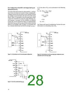
ing the RESET pin low, the input (V ) switching signals
IN
must be configured for an output (V ) low state. This
OL
can be handled directly by the microcontroller or by
hardwiring to synchronize the RESET signal with the ap-
propriate input signal. Figure 73a shows how to connect
the RESET to the V signal for safe automatic reset in
IN+
the noninverting input configuration. Figure 73b shows
how to configure the V /RESET signals so that a RESET
IN+
signal from the microcontroller causes the input to be
in the “output-off” state. Similarly, Figures 73c and 73d
show automatic RESET and microcontroller RESET safe
configurations for the inverting input configuration.
HCPL-316J
HCPL-316J
1
2
3
4
5
6
7
8
V
V
V
IN+
IN-
1
2
3
4
5
6
7
8
V
V
V
IN+
IN-
CC1
+
–
CC1
µC
+
–
µC
GND1
GND1
RESET
FAULT
RESET
FAULT
V
V
LED1+
LED1-
V
V
LED1+
LED1-
CONNECT
TO OTHER
RESETS
CONNECT
TO OTHER
FAULTS
Figure 72. Auto-reset configuration.
Figure 71. Global-shutdown, global reset configuration.
HCPL-316J
HCPL-316J
V
IN+
1
2
3
4
5
6
7
8
V
V
V
1
2
3
4
5
6
7
8
V
V
V
IN+
IN-
IN+
IN-
V
V
CC
CC
CC1
CC1
µC
µC
GND1
GND1
V
/
IN+
RESET
RESET
FAULT
RESET
FAULT
RESET
FAULT
FAULT
V
V
LED1+
LED1+
V
V
LED1-
LED1-
Figure 73a. Safe hardware reset for noninverting input
configuration (automatically resets for every VIN+ input).
Figure 73b. Safe hardware reset for noninverting input
configuration.
27

 AVAGO [ AVAGO TECHNOLOGIES LIMITED ]