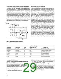
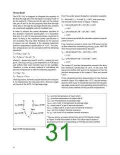
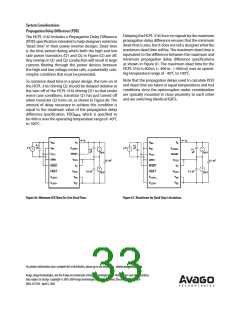
Thermal Model
From the earlier power dissipation calculation example:
P = 90.8mW, P = 314mW, T = 100°C, and assuming
the thermal model shown in Figure 77 below.
The HCPL-316J is designed to dissipate the majority of
the heat through pins 4 for the input IC and pins 9 and 10
i
o
A
for the output IC. (There are two V pins on the output
EE
side, pins 9 and 10, for this purpose.) Heat flow through
other pins or through the package directly into ambient
are considered negligible and not modeled here.
T
ji
= (90.8mW)(60°C/W + 50°C/W) + 100°C
= 110°C
In order to achieve the power dissipation specified in
the absolute maximum specification, it is imperative
that pins 4, 9, and 10 have ground planes connected to
them. As long as the maximum power specification is
not exceeded, the only other limitation to the amount
of power one can dissipate is the absolute maximum
junction temperature specification of 125°C. The junc-
tion temperatures can be calculated with the following
equations:
T
= (240mW)(30°C/W + 50°C/W) + 100°C
= 119°C
jo
both of which are within the absolute maximum specifi-
cation of 125°C.
If we, however, assume a worst case PCB layout and no
air flow where the estimated q and q
Then the junction temperatures become
are 100°C/W.
4A
9,10A
T
ji
= (90.8mW)(60°C/W + 100°C/W) + 100°C
T = P (q + q ) + T
ji
i
i4
4A
A
= 115°C
T
= P (q
+ q ) + T
9,10A A
jo
o
o9,10
T
jo
= (240mW)(30°C/W + 100°C/W) + 100°C
= 131°C
where P = power into input IC and P = power into out-
i
o
put IC. Since q and q
are dependent on PCB layout
4A
9,10A
and airflow, their exact number may not be available.
Therefore, a more accurate method of calculating the
junction temperature is with the following equations:
The output IC junction temperature exceeds the abso-
lute maximum specification of 125°C. In this case, PCB
layout and airflow will need to be designed so that the
junction temperature of the output IC does not exceed
125°C.
T = P q + T
ji
i i4
P4
T
= P q
+ T
jo
o o9,10 P9,10
If the calculated junction temperatures for the thermal
model in Figure 78 is higher than 125°C, the pin temper-
ature for pins 9 and 10 should be measured (at the pack-
age edge) under worst case operating environment for a
more accurate estimate of the junction temperatures.
These equations, however, require that the pin 4 and pins
9, 10 temperatures be measured with a thermal couple
on the pin at the HCPL-316J package edge.
T = junction temperature of input side IC
ji
T
T
T
q
q
q
q
= junction temperature of output side IC
= pin 4 temperature at package edge
jo
T
T
jo
ji
P4
= pin 9 and 10 temperature at package edge
P9,10
θ
= 60°C/W
θ
= 30°C/W
O9,10
i4
= input side IC to pin 4 thermal resistance
I4
= output side IC to pin 9 and 10 thermal resistance
I9,10
T
T
P9,10
P4
= pin 4 to ambient thermal resistance
4A
= pin 9 and 10 to ambient thermal resistance
9,10A
θ
= 50°C/W*
θ
= 50°C/W*
9,10A
4A
T
A
*The q and q
values shown here are for PCB layouts shown
9,10A
4A
in Figure 78 with reasonable air flow. This value may increase or
decrease by a factor of 2 depending on PCB layout and/or airflow.
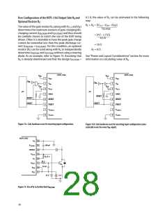
Figure 78. HCPL-316J thermal model.
31

 AVAGO [ AVAGO TECHNOLOGIES LIMITED ]