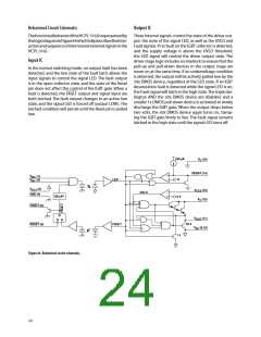
0.5 A, the value of R can be estimated in the following
way:
User-Configuration of the HCPL-316J Output Side R and
C
G
Optional Resistor R :
C
R + R = [V – V – (V )]
C
G
CC2
OH
EE
The value of the gate resistor R (along withV andV )
EE
G
CC2
I
OH,PEAK
determines the maximum amount of gate-charging/dis-
charging current (I and I ) and thus should
ON,PEAK
OFF,PEAK
= [4 V – (-5 V)]
0.5 A
be carefully chosen to match the size of the IGBT being
driven. Often it is desirable to have the peak gate charge
current be somewhat less than the peak discharge cur-
= 18 Ω
rent (I
< I
). For this condition, an optional
ON,PEAK
OFF,PEAK
resistor (R ) can be used along with R to independently
R = 8 Ω
C
C
G
determine I
and I
without using a steering
ON,PEAK
OFF,PEAK
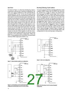
diode. As an example, refer to Figure 74. Assuming that
is already determined and that the design I
See “Power and Layout Considerations”section for more
information on calculating value of R .
R
=
G
OH,PEAK
G
HCPL-316J
HCPL-316J
V
V
V
V
CC
CC
CC
CC
1
2
3
4
5
6
7
8
V
V
V
1
2
3
4
5
6
7
8
V
V
V
IN+
IN-
IN+
IN-
V
IN-
V
IN-
CC1
CC1
µC
µC
GND1
GND1
RESET
RESET
FAULT
RESET
FAULT
RESET
FAULT
FAULT
V
V
V
V
LED1+
LED1-
LED1+
LED1-
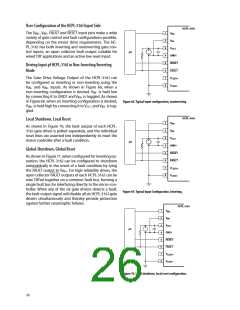
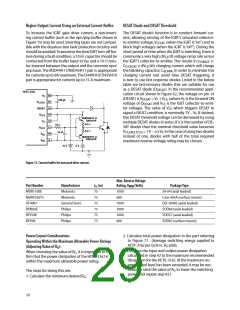
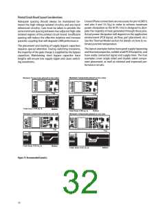
Figure 73c. Safe hardware reset for inverting input configuration.
Figure 73d. Safe hardware reset for inverting input configuration (auto-
matically resets for every VIN- input).
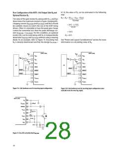
HCPL-316J
V
16
15
E
V
100 pF
LED2+
DESAT 14
V
13
12
11
10
9
CC2
R
8 Ω
C
V
C
10 Ω
10 nF
V
OUT
V
V
EE
EE
15 V
-5 V
Figure 74. Use of RC to further limit ION,PEAK
.
28

 AVAGO [ AVAGO TECHNOLOGIES LIMITED ]