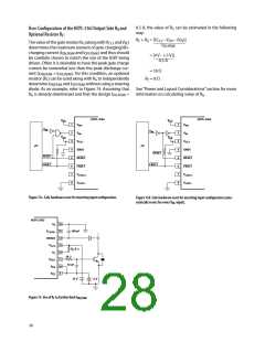
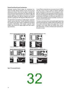
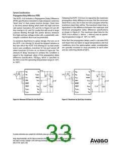
Printed Circuit Board Layout Considerations
Ground Plane connections are necessary for pin 4 (GND1)
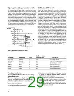
Adequate spacing should always be maintained be-
tween the high voltage isolated circuitry and any input
referenced circuitry. Care must be taken to provide the
same minimum spacing between two adjacent high-side
isolated regions of the printed circuit board. Insufficient
spacing will reduce the effective isolation and increase
parasitic coupling that will degrade CMR performance.
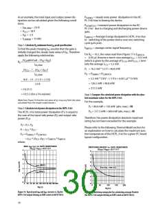
and pins 9 and 10 (V ) in order to achieve maximum
EE
power dissipation as the HCPL-316J is designed to dissi-
pate the majority of heat generated through these pins.
Actual power dissipation will depend on the application
environment (PCB layout, air flow, part placement, etc.)
See the Thermal Model section for details on how to es-
timate junction temperature.
The placement and routing of supply bypass capacitors
requires special attention. During switching transients,
the majority of the gate charge is supplied by the bypass
capacitors. Maintaining short bypass capacitor trace
lengths will ensure low supply ripple and clean switch-
ing waveforms.
The layout examples below have good supply bypassing
and thermal properties, exhibit small PCB footprints, and
have easily connected signal and supply lines. The four
examples cover single sided and double sided compo-
nent placement, as well as minimal and improved per-
formance circuits.
Figure 79. Recommended layout(s).
32

 AVAGO [ AVAGO TECHNOLOGIES LIMITED ]