As an example, the total input and output power dis-
sipation can be calculated given the following condi-
tions:
P
= steady-state power dissipation in the HC-
O(BIAS)
PL-316J due to biasing the device.
P
= transient power dissipation in the HC-
O(SWITCH)
• I
~ 2.0 A
ON, MAX
PL-316J due to charging and discharging power device
gate.
• V
= 18 V
CC2
• V = -5 V
EE
E
= Average Energy dissipated in HCPL-316J due
SWITCH
• f
= 15 kHz
CARRIER
to switching of the power device over one switching
cycle (µJ/cycle).
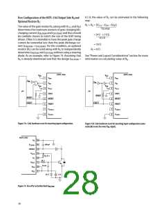
Step 1: Calculate R minimum from I peak specification:
To find the peak charging l assume that the gate is
G
OL
f
= average carrier signal frequency.
SWITCH
OL
initially charged the steady-state value of V . Therefore
apply the following relationship:
EE
For R = 10.5, the value read from Figure 77 is E
G
SWITCH
=
6.05 µJ. Assume a worst-case average I
= 16.5 mA
CC1L
CC1
[V @650 µA – (V +V )]
OH
OL EE
(which is given by the average of I
and I
). Simi-
CC1H
R = ——————————
G
larly the average I
= 5.5 mA.
CC2
I
OL,PEAK
P
P
= 16.5 mA * 5.5 V = 90.8 mW
I
[V – 1 – (V + V )]
CC2
OL
EE
= —————————
= P
+ P
O,SWITCH
O
O(BIAS)
I
OL,PEAK
= 5.5 mA * (18 V – (–5 V)) + 6.051 µJ * 15 kHz
= 126.5 mW + 90.8 mW
18 V – 1 V – (1.5 V + (‑5 V))
= ——————————
2.0 A
= 217.3 mW
= 10.25 W
≈ 10.5 W (for a 1% resistor)
Step 3: Compare the calculated power dissipation with the abso-
lute maximum values for the HCPL-316J:
For the example,
(Note from Figure 76 that the real value of I may vary from the value
calculated from the simple model shown.)
OL
P = 90.8 mW < 150 mW (abs. max.) ) OK
I
Step 2: Calculate total power dissipation in the HCPL-316J:
P
= 217.3 mW < 600 mW (abs. max.) ) OK
O
The HCPL-316J total power dissipation (P ) is equal to
T
the sum of the input-side power (P ) and output-side
I
Therefore, the power dissipation absolute maximum
rating has not been exceeded for the example.
power (P ):
O
P = P + P
O
T
I
Please refer to the following Thermal Model section for
an explanation on how to calculate the maximum junc-
tion temperature of the HCPL-316J for a given PC board
layout configuration.
P = I * V
I
CC1
CC1
P
O
= P
+ P
O(BIAS) O,SWTICH
= I * (V –V ) + E * f
SWITCH SWITCH
CC2
CC2 EE
where,
MAX. I , I
ON OFF
vs. GATE RESISTANCE
= 25 V / 5 V
SWITCHING ENERGY vs. GATE RESISTANCE
(V / V
CC2
EE2
(V
/ V
= 25 V / 5 V
CC2
EE2
4
9
8
7
6
5
4
3
2
3
2
1
I
I
(MAX.)
OFF
Ess (Qg = 650 nC)
0
(MAX.)
ON
-1
-2
-3
1
0
0
20 40 60 80 100120140160180 200
0
50
100
150
200
Rg (Ω)
Rg (Ω)
Figure 76. Typical peak ION and IOFF currents vs. Rg (for
HCPL-316J output driving an IGBT rated at 600 V/100 A.
Figure 77. Switching energy plot for calculating average Pswitch
(for HCPL-316J output driving an IGBT rated at 600 V/100 A).
30

 AVAGO [ AVAGO TECHNOLOGIES LIMITED ]