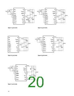
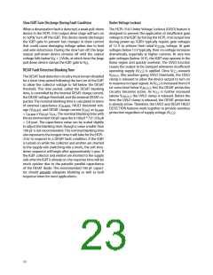
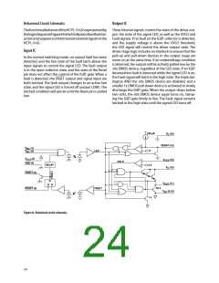
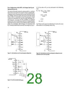
Behavioral Circuit Schematic
Output IC
ThefunctionalbehavioroftheHCPL-316Jisrepresentedby
thelogicdiagraminFigure64whichfullydescribestheinter-
actionandsequenceofinternalandexternalsignalsinthe
HCPL-316J.
Three internal signals control the state of the driver out-
put: the state of the signal LED, as well as the UVLO and
Fault signals. If no fault on the IGBT collector is detected,
and the supply voltage is above the UVLO threshold,
the LED signal will control the driver output state. The
driver stage logic includes an interlock to ensure that the
pull-up and pull-down devices in the output stage are
never on at the same time. If an undervoltage condition
is detected, the output will be actively pulled low by the
50x DMOS device, regardless of the LED state. If an IGBT
desaturation fault is detected while the signal LED is on,
the Fault signal will latch in the high state. The triple dar-
lington AND the 50x DMOS device are disabled, and a
smaller 1x DMOS pull-down device is activated to slowly
discharge the IGBT gate. When the output drops below
two volts, the 50x DMOS device again turns on, clamp-
ing the IGBT gate firmly to Vee. The Fault signal remains
latched in the high state until the signal LED turns off.
Input IC
In the normal switching mode, no output fault has been
detected, and the low state of the fault latch allows the
input signals to control the signal LED. The fault output
is in the open-collector state, and the state of the Reset
pin does not affect the control of the IGBT gate. When a
fault is detected, the FAULT output and signal input are
both latched. The fault output changes to an active low
state, and the signal LED is forced off (output LOW). The
latched condition will persist until the Reset pin is pulled
low.
250 µA
V
(16)
E
DESAT (14)
+
–
V
V
(1)
(2)
IN+
IN–
LED
7 V
V
(3)
CC1
V
(13)
(12)
CC2
–
+
UVLO
GND (4)
DELAY
12 V
V
C
FAULT (6)
Q
V
(11)
OUT
R
S
50 x
RESET (5)
FAULT
V
(9,10)
EE
1 x
Figure 64. Behavioral circuit schematic.
24

 AVAGO [ AVAGO TECHNOLOGIES LIMITED ]