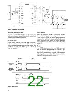
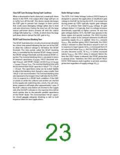
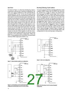
Slow IGBT Gate Discharge During Fault Condition
Under Voltage Lockout
When a desaturation fault is detected, a weak pull-down
device in the HCPL-316J output drive stage will turn on
to ‘softly’ turn off the IGBT. This device slowly discharges
the IGBT gate to prevent fast changes in drain current
that could cause damaging voltage spikes due to lead
and wire inductance. During the slow turn off, the large
output pull-down device remains off until the output
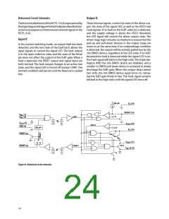
The HCPL-316J Under Voltage Lockout (UVLO) feature is
designed to prevent the application of insufficient gate
voltage to the IGBT by forcing the HCPL-316J output low
during power-up. IGBTs typically require gate voltages
of 15 V to achieve their rated V
voltage. At gate
CE(ON)
voltages below 13 V typically, their on-voltage increases
dramatically, especially at higher currents. At very low
gate voltages (below 10 V), the IGBT may operate in the
linear region and quickly overheat. The UVLO function
causes the output to be clamped whenever insufficient
voltage falls below V + 2 Volts, at which time the large
EE
pull down device clamps the IGBT gate to V
.
EE
DESAT Fault Detection Blanking Time
operating supply (V ) is applied. Once V
exceeds
CC2
CC2
V
(the positive-going UVLO threshold), the UVLO
UVLO+
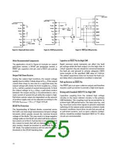
The DESAT fault detection circuitry must remain disabled
for a short time period following the turn-on of the IGBT
to allow the collector voltage to fall below the DESAT
theshold. This time period, called the DESAT blanking
time, is controlled by the internal DESAT charge current,
the DESAT voltage threshold, and the external DESAT ca-
pacitor. The nominal blanking time is calculated in terms
clamp is released to allow the device output to turn on
in response to input signals. As V is increased from 0 V
CC2
(at some level below V
circuitry becomes active. As V
), first the DESAT protection
UVLO+
is further increased
CC2
(above V
), the UVLO clamp is released. Before the
UVLO+
time the UVLO clamp is released, the DESAT protection
is already active. Therefore, the UVLO and DESAT FAULT
DETECTION features work together to provide seamless
of external capacitance (C
), FAULT threshold volt-
BLANK
age (V
), and DESAT charge current (I
) as t
CHG BLANK
DESAT
protection regardless of supply voltage (V ).
CC2
= C
x V
/I
. The nominal blanking time with
BLANK
DESAT CHG
therecommended100pFcapacitoris100pF*7V/250µA
= 2.8 µsec. The capacitance value can be scaled slightly
to adjust the blanking time, though a value smaller than
100 pF is not recommended. This nominal blanking time
also represents the longest time it will take for the HCPL-
316J to respond to a DESAT fault condition. If the IGBT
is turned on while the collector and emitter are shorted
to the supply rails (switching into a short), the soft shut-
down sequence will begin after approximately 3 µsec. If
the IGBT collector and emitter are shorted to the supply
rails after the IGBT is already on, the response time will be
much quicker due to the parasitic parallel capacitance
of the DESAT diode. The recommended 100 pF capaci-
tor should provide adequate blanking as well as fault
response times for most applications.
23

 AVAGO [ AVAGO TECHNOLOGIES LIMITED ]