HCPL-316J
1
2
3
4
5
6
7
8
V
V
V
V
16
15
IN+
IN-
E
0.1
µF
0.1
µF
100 pF
V
LED2+
D
DESAT
100 Ω
DESAT 14
CC1
+
–
5 V
+
–
0.1
µF
µC
V
F
GND1
V
13
12
11
10
9
CC2
3.3
kΩ
Q1
Q2
V
= 18 V
CC2
+
–
+
–
RESET
FAULT
V
C
V
CE
R
g
V
OUT
0.1
µF
3-PHASE
OUTPUT
47
kΩ
V
V
V
V
LED1+
LED1-
EE
EE
330 pF
+
–
+
–
V
= -5 V
EE
V
CE
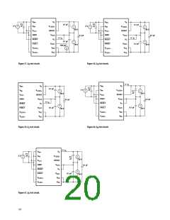
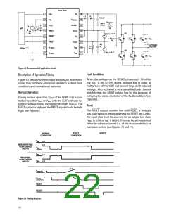
Figure 62. Recommended application circuit.
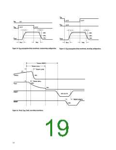
Fault Condition
Description of Operation/Timing
When the voltage on the DESAT pin exceeds 7V while
the IGBT is on, V is slowly brought low in order to
“softly”turn-off the IGBT and prevent large di/dt induced
voltages. Also activated is an internal feedback channel
which brings the FAULT output low for the purpose of
notifying the micro-controller of the fault condition. See
Figure 63.
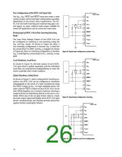
Figure 63 below illustrates input and output waveforms
under the conditions of normal operation, a desat fault
condition, and normal reset behavior.
OUT
Normal Operation
During normal operation, V
of the HCPL-316J is con-
OUT
trolled by either V or V , with the IGBT collector-to-
IN+
IN-
emitter voltage being monitored through D
FAULT output is high and the RESET input should be held
high. See Figure63.
. The
DESAT
Reset
The FAULT output remains low until RESET is brought
low. See Figure 63. While asserting the RESET pin (LOW),
the input pins must be asserted for an output low state
(V is LOW or V is HIGH). This may be accomplished
IN+
IN-
either by software control (i.e. of the microcontroller) or
hardware control (see Figures 73 and 74).
NORMAL
OPERATION
FAULT
CONDITION
RESET
V
IN-
IN+
IN-
0 V
5 V
NON-INVERTING
CONFIGURED
INPUTS
V
V
V
5 V
INVERTING
CONFIGURED
INPUTS
IN+ 5 V
7 V
V
V
DESAT
OUT
FAULT
RESET
Figure 63. Timing diagram.
22

 AVAGO [ AVAGO TECHNOLOGIES LIMITED ]