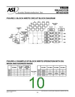
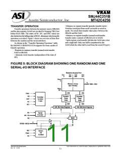
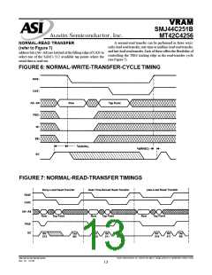
VRAM
SMJ44C251B
MT42C4256
Austin Semiconductor, Inc.
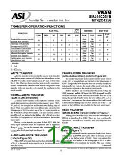
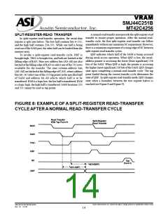
A normal-read transfer must precede the split-register-read
transfer to ensure proper operation. After the normal-read-
transfer cycle, the first split-register read transfer can follow
immediately without any minimum SC requirement. However,
there is a minimum requirement of a rising edge of SC between
split-register read-transfer cycles.
SPLIT-REGISTER-READ TRANSFER
In split-register-read-transfer operation, the serial-data
register is split into halves. The low half contains bits 0–255,
and the high half contains 256–511. While one half is being
read out of the SAM port, the other half can be loaded from the
memory array.
QSF indicates which half of the SAM is being accessed
during serial-access operation. When QSF is low, the serial-
address pointer is accessing the lower (least significant) 256
bits of the SAM. When QSF is high, the pointer is accessing
the higher (most significant) 256 bits of the SAM. QSF changes
state upon completing a normal-read-transfer cycle. The tap
point loaded during the current transfer cycle determines the
state of QSF. In split-register read-transfer mode, QSF changes
state when a boundary between the two register halves is
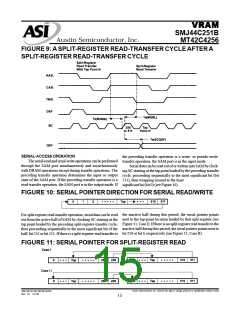
reached (see Figure 8 and Figure 9).
To invoke a split-register read-transfer cycle, DSF is
brought high, TRG\ is brought low, and both are latched at the
falling edge of RAS\. Nine row-address bits (A0–A8) are also
latched at the falling edge of RAS\ to select one of the 512 rows
available for the transfer. The nine column-address bits
(A0–A8) are latched at the falling edge of CAS\, where address
bitsA0 –A7 select one of the 255 tap points in the specified half
of SAM and address bit A8 selects which half is to be
transferred. IfA8 is a logic low, the low half is transferred. IfA8
is a logic high, the high half is transferred. SAM locations 255
and 511 cannot be used as tap points.
FIGURE 8: EXAMPLE OFA SPLIT-REGISTER READ-TRANSFER
CYCLEAFTER ANORMAL READ-TRANSFER CYCLE
Austin Semiconductor, Inc. reserves the right to change products or specifications without notice.
SMJ44C251B/MT42C4256
Rev. 0.1 12/03
14

 AUSTIN [ AUSTIN SEMICONDUCTOR ]