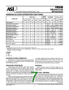
VRAM
SMJ44C251B
MT42C4256
Austin Semiconductor, Inc.
• Memory-to-register transfer (pseudo-transfer write).
Switches serial port from serial-out mode to serial-in
mode. No actual data transfer takes place between the
DRAM and the SAM.
• Memory-to-register transfer (normal-read transfer,
transfer entire contents of DRAM row to SAM)
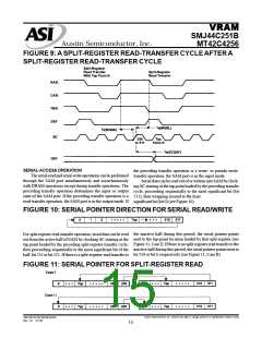
• Split-register-read transfer (divides the SAM into a low
and a high half. Only one half is transferred to the
SAM while the other half is read from the serial I/O port.)
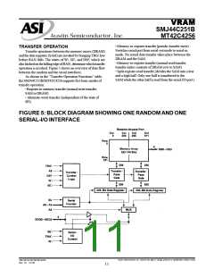
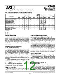
TRANSFER OPERATION
Transfer operations between the memory arrays (DRAM)
and the data registers (SAM) are invoked by bringing TRG\ low
before RAS\ falls. The states of W\, SE\, and DSF, which are
also latched on the falling edge of RAS\, determine which transfer
operation is invoked. Figure 5 shows an overview of data flow
between the random and the serial interfaces.
As shown in the “Transfer-Operation Functions” table,
the SMJ44C251B/MT42C4256 supports five basic modes of
transfer operation:
• Register-to-memory transfer (normal write transfer,
SAM to DRAM)
• Alternate-write transfer (independent of the state of
SE\)
FIGURE 5: BLOCK DIAGRAM SHOWING ONE RANDOMAND ONE
SERIAL-I/O INTERFACE
Austin Semiconductor, Inc. reserves the right to change products or specifications without notice.
SMJ44C251B/MT42C4256
Rev. 0.1 12/03
11

 AUSTIN [ AUSTIN SEMICONDUCTOR ]