VRAM
SMJ44C251B
MT42C4256
Austin Semiconductor, Inc.
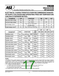
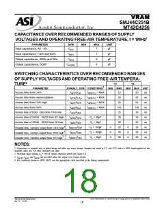
CAPACITANCE OVER RECOMMENDED RANGES OF SUPPLY
VOLTAGES AND OPERATING FREE-AIR TEMPERATURE, f = 1MHz1
PARAMETER
SYM
MIN
MAX
UNIT
Input capacitance, A0 - A8
C
i(A)
7
pF
Input capacitance, CAS\ and RAS\
Output capacitance, SDQs and DQs
Output capacitance, SQSF
C
7
9
9
pF
pF
pF
i(RC)
C
o(O)
C
o(QSF)
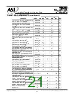
SWITCHING CHARACTERISTICS OVER RECOMMENDED RANGES
OF SUPPLY VOLTAGESAND OPERATING FREE-AIR TEMPERA-
TURE2
-10
-12
4
PARAMETER
SYM/ALT. SYM CONDITIONS
MIN MAX
MIN MAX UNIT
Access time from CAS\
t
/t
t
t
t
t
= MAX
= MAX
= MAX
= MAX
25
30
60
65
120
30
35
25
20
20
20
ns
ns
ns
ns
ns
ns
ns
ns
ns
ns
a(C) CAC
d(RLCL)
d(RLCL)
d(RLCL)
d(RLCL)
Access time from column address
Access time from CAS\ high
t
/t
50
55
a(CA) CAA
t
/t
a(CP) CPA
Access time from RAS\
t
/t
100
25
a(R) RAC
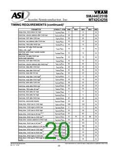
Access time of DQ0 - DQ3 from TRG\ low
Access time of SDQ0 - SDQ3 from SC high
Access time of SDQ0 - SDQ3 from SE\ low
t
/t
a(G) OEA
t
/t
C = 30pF
30
a(SQ) SCA
L
t
/t
C = 30pF
20
a(SE) SEA
L
3
t
/t
C = 100pF
0
0
0
20
20
20
0
0
0
dis(CH) OFF
L
Disable time, random output from CAS\ high
3
t
/t
C = 100pF
L
dis(G) OEZ
Disable time, random output from TRG\ high
3
t
/t
C = 30pF
L
dis(SE) SEZ
Disable time, random output from SE\ high
NOTES:
1. Capacitance is sampled only at initial design and after any major change. Samples are tested at 0 V and 25°C with a 1-MHz signal applied to the
terminal under test. All other terminals are open.
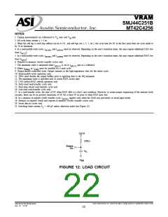
2. Switching times assume CL = 100 pF unless otherwise noted (see Figure 12).
3. tdis(CH), tdis(G), and tdis(SE) are specified when the output is no longer driven.
4. For conditions shown as MIN/ MAX, use the appropriate value specified in the timing requirements.
Austin Semiconductor, Inc. reserves the right to change products or specifications without notice.
SMJ44C251B/MT42C4256
Rev. 0.1 12/03
18

 AUSTIN [ AUSTIN SEMICONDUCTOR ]