VRAM
SMJ44C251B
MT42C4256
Austin Semiconductor, Inc.
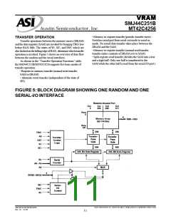
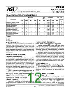
TRANSFER-OPERATION FUNCTIONS
CAS\
FALL
RAS\ FALL
FUNCTION
ADDRESS
DQ0 - DQ3
CAS\
CAS\
TRG\
W\
DSF
X
SE\
L
DSF
X
RAS\
CAS\
RAS\
W\
Register-to-memory transfer
(normal write transfer)
Alternate-write transfer
(independent of SE\)
Serial-write-mode enable
(pseudo-transfer write)
Memory-to-register transfer
(normal read transfer)
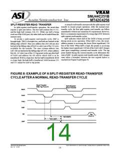
Split-register-read transfer
(must reload tap)
Row
Addr
Row
Addr
Refresh
Addr
Row
Addr
Row
Addr
Tap
Point
Tap
Point
Tap
Point
Tap
Point
Tap
H
L
L
L
L
L
L
X
X
X
X
X
X
H
L
H
X
X
X
X
X
X
H
L
L
H
X
H
H
H
L
X
X
H
H
X
X
Point
LEGEND:
H = High
L = Low
X = Don’t Care
PSEUDO-WRITE TRANSFER
WRITE TRANSFER
All write-transfer cycles (except the pseudo write transfer)
transfer the entire content of SAM to the selected row in the
DRAM. To invoke a write-transfer cycle, W\ must be low when
RAS\ falls. There are three possible write-transfer operations:
normal-write transfer, alternate-write transfer, and pseudo-write
transfer. All write-transfer cycles switch the serial port to the
serial-in mode.
(write-mode control) (refer to Figure 28)
To invoke the pseudo-write transfer (write-mode control
cycle), SE\ is brought high and latched at the falling edge of
RAS\. The pseudo-write transfer does not actually invoke any
data transfer but switches the mode of the serial port from the
serial-out (read) mode to the serial-in (write) mode.
Before serial data can be clocked into the serial port via the
SDQ terminals and the SC input, the SDQ terminals must be
switched into input mode. Because the transfer does not occur
during the pseudo-transfer write, the row address (A0–A8) is
in the don’t care state and the column address (A0–A8), which
is latched on the falling edge of CAS\, selects one of the 512 tap
points in the SAM that are available for the next serial input.
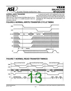
NORMAL-WRITE TRANSFER
(SAM-to-DRAM transfer)
A normal-write transfer cycle loads the contents of the
serial-data register to a selected row in the memory array. TRG\,
W\, and SE\ are brought low and latched at the falling edge of
RAS\. Nine row-address bits (A0–A8) are also latched at the
falling edge of RAS\ to select one of the 512 rows available as READ TRANSFER
the destination of the data transfer. The nine column-address
(DRAM-to-SAM transfer) (refer to Figure 7)
bits (A0–A8) are latched at the falling edge of CAS\ to select
one of the 512 tap points in SAM that are available for the next
serial input.
During a write-transfer operation before RAS\ falls, the
serial-input operation must be suspended after a minimum
During a read-transfer cycle, data from the selected row in
DRAM is transferred to SAM. There are two read-transfer
operations: normal-read transfer and split-register-read
transfer.
delay of td(SCRL) but can be resumed after a minimum delay of
td(RHSC) after RAS goes high (see Figure 6).
NORMAL-READ TRANSFER
(refer to Figure 7)
The normal-read-transfer operation loads data from a
selected row in DRAM into SAM. TRG\ is brought low and
latched at the falling edge of RAS\. Nine row-address bits
(A0–A8) are also latched at the falling edge of RAS\ to select
one of the 512 rows available for transfer. The nine column-
(continued)
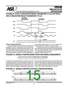
ALTERNATE-WRITE TRANSFER
(refer to Figure 30)
When DSF is brought high and latched at the falling edge
of RAS\ in the normal-write-transfer cycle, the alternate-write
transfer occurs.
Austin Semiconductor, Inc. reserves the right to change products or specifications without notice.
SMJ44C251B/MT42C4256
Rev. 0.1 12/03
12

 AUSTIN [ AUSTIN SEMICONDUCTOR ]