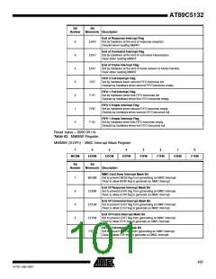
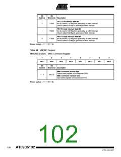
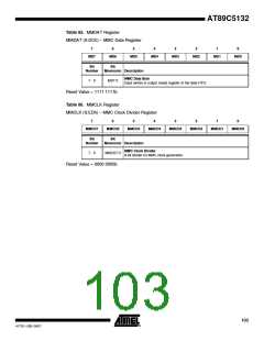
AT89C5132
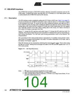
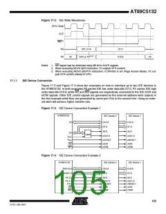
Figure 17-2. IDE Write Waveforms
CPU Clock
ALE
WR(1)
DPL or Ri
D7:0
P0
P2
P2
DPH or P2(2),(3)
D15:8
P2
Notes: 1. WR signal may be stretched using M0 bit in AUXR register.
2. When executing MOVX @Ri instruction, P2 outputs SFR content.
3. When executing MOVX @DPTR instruction, if DPHDIS is set (Page Access Mode), P2 out-
puts SFR content instead of DPH.
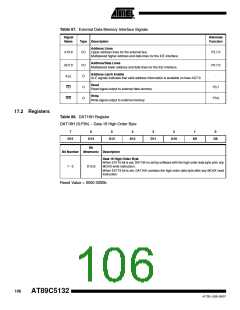
17.1.1
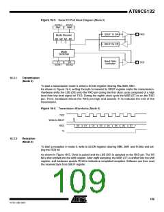
IDE Device Connection
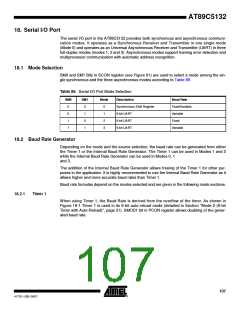
Figure 17-3 and Figure 17-4 show two examples on how to interface up to two IDE devices to
the AT89C5132. In both examples P0 carries IDE low order data bits D7:0, P2 carries IDE high
order data bits D15:8, while RD and WR signals are respectively connected to the IDE nIOR and
nIOW signals. Other IDE control signals are generated by the external address latch outputs in
the first example while they are generated by some port I/Os in the second one. Using an exter-
nal latch will achieve higher transfer rate.
Figure 17-3. IDE Device Connection Example 1
AT89C5132
IDE Device 0
IDE Device 1
P2
D15-8
D7:0
A2:0
D15-8
D7:0
A2:0
P0
Latch
nCS1:0
nCS1:0
ALE
Px.y
nRESET
nRESET
RD
nIOR
nIOW
nIOR
nIOW
WR
Figure 17-4. IDE Device Connection Example 2
AT89C5132
IDE Device 0
IDE Device 1
P2/A15:8
P0/AD7:0
D15-8
D7:0
D15-8
D7:0
P4.2:0
P4.4:3
P4.5
RD
A2:0
A2:0
nCS1:0
nRESET
nIOR
nCS1:0
nRESET
nIOR
WR
nIOW
nIOW
105
4173E–USB–09/07

 ATMEL [ ATMEL ]