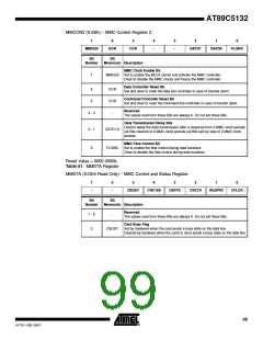
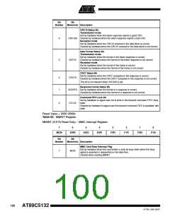
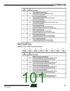
PDF
最近搜索
热门搜索
发布采购

| 型号: | 895132-UL |
| PDF下载: | 下载PDF文件 查看货源 |
| 内容描述: | USB微控制器,带有64K字节Flash存储器 [USB Microcontroller with 64K Bytes Flash Memory] |
| 分类和应用: | 存储微控制器 |
| 文件页数/大小: | 182 页 / 1660 K |
| 品牌: |  ATMEL [ ATMEL ] ATMEL [ ATMEL ] |
专业IC领域供求交易平台:提供全面的IC Datasheet资料和资讯,Datasheet 1000万数据,IC品牌1000多家。