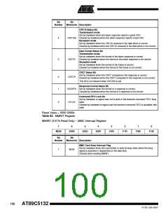
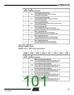
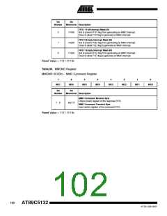
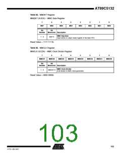
17. IDE/ATAPI Interface
The AT89C5132 provide an IDE/ATAPI interface allowing connection of devices such as CD-
ROM reader, CompactFlash cards, hard disk drive, etc. It consists of a 16-bit data transfer (read
or write) between the AT89C5132 and the IDE devices.
17.1 Description
The IDE interface mode is enabled by setting the EXT16 bit in AUXR (see Table 14 on page 27).
As soon as this bit is set, all MOVX instructions read or write are done in a 16-bit mode compare
to the standard 8-bit mode. P0 carries the low order multiplexed address and data bus (A7:0,
D7:0) while P2 carries the high order multiplexed address and data bus (A15:8, D15:8). When
writing data in IDE mode, the ACC contains D7:0 data (as in 8-bit mode) while DAT16H register
(see Table 88) contains D15:8 data. When reading data in IDE mode, D7:0 data is returned in
ACC while D15:8 data is returned in DAT16H.
Figure 17-1 shows the IDE read bus cycle while Figure 17-2 shows the IDE write bus cycle. For
simplicity, these figures depict the bus cycle waveforms in idealized form and do not provide pre-
cise timing information. For IDE bus cycle timing parameters refer to the Section “AC
Characteristics”.
IDE cycle takes 6 CPU clock periods which is equivalent to 12 oscillator clock periods in stan-
dard mode or 6 oscillator clock periods in X2 mode. For further information on X2 mode, refer to
the Section “X2 Feature”, page 12.
Slow IDE devices can be accessed by stretching the read and write cycles. This is done using
the M0 bit in AUXR. Setting this bit changes the width of the RD and WR signals from 3 to 15
CPU clock periods.
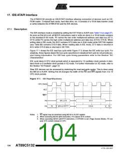
Figure 17-1. IDE Read Waveforms
CPU Clock
ALE
RD(1)
DPL or Ri
D7:0
P0
P2
P2
DPH or P2(2),(3)
D15:8
P2
Notes: 1. RD signal may be stretched using M0 bit in AUXR register.
2. When executing MOVX @Ri instruction, P2 outputs SFR content.
3. When executing MOVX @DPTR instruction, if DPHDIS is set (Page Access Mode), P2 out-
puts SFR content instead of DPH.
104
AT89C5132
4173E–USB–09/07

 ATMEL [ ATMEL ]