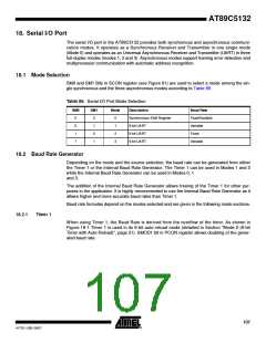
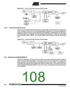
Figure 18-1. Timer 1 Baud Rate Generator Block Diagram
PER
CLOCK
÷ 6
0
1
Overflow
TL1
(8 bits)
÷ 2
0
1
To serial
Port
T1
C/T1#
TMOD.6
SMOD1
PCON.7
INT1
TH1
(8 bits)
GATE1
TMOD.7
T1
CLOCK
TR1
TCON.6
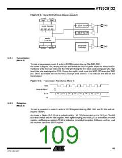
18.2.2
Internal Baud Rate Generator
When using the Internal Baud Rate Generator, the Baud Rate is derived from the overflow of the
timer. As shown in Figure 18-2, the Internal Baud Rate Generator is an 8-bit auto-reload timer
feed by the peripheral clock or by the peripheral clock divided by 6 depending on the SPD bit in
BDRCON register (see Table 95). The Internal Baud Rate Generator is enabled by setting BBR
bit in BDRCON register. SMOD1 bit in PCON register allows doubling of the generated baud
rate.
Figure 18-2. Internal Baud Rate Generator Block Diagram
PER
CLOCK
÷ 6
0
1
Overflow
BRG
(8 bits)
÷ 2
0
1
To serial
Port
SPD
BDRCON.1
BRR
BDRCON.4
SMOD1
PCON.7
To serial
Port (M0)
BRL
(8 bits)
IBRG
CLOCK
IBRG0
CLOCK
18.3 Synchronous Mode (Mode 0)
Mode 0 is a half-duplex, synchronous mode, which is commonly used to expand the I/0 capabil-
ities of a device with shift registers. The transmit data (TXD) pin outputs a set of eight clock
pulses while the receive data (RXD) pin transmits or receives a byte of data. The 8-bit data are
transmitted and received least-significant bit (LSB) first. Shifts occur at a fixed Baud Rate (see
Section "Baud Rate Selection (Mode 0)", page 110). Figure 18-3 shows the serial port block dia-
gram in Mode 0.
108
AT89C5132
4173E–USB–09/07

 ATMEL [ ATMEL ]